Planar integrated circuit including a plasmon waveguide-fed Schottky barrier detector and transistors connected therewith

a technology of integrated circuits and transistors, which is applied in the direction of instruments, lighting and heating apparatus, optical elements, etc., can solve the problems of difficult inability to use schottky detectors for optical communication, and inability to achieve the optimization of photon absorption in schottky electrodes, etc., to achieve the effect of reducing power consumption and facilitating waveguide/detector structures

Inactive Publication Date: 2007-01-30
APPLIED MATERIALS INC
View PDF20 Cites 31 Cited by
  • Summary
  • Abstract
  • Description
  • Claims
  • Application Information

AI Technical Summary

Benefits of technology

[0010]A waveguide medium and Schottky barrier detector integrated with the waveguide medium are buried inside a semiconductor substrate of a planar integrated circuit, so that the integrated waveguide and Schottky barrier detector are generally below or co-planar with the plane of the substrate, thus providing a planar integrated circuit structure. The waveguide medium can be surrounded by a wall having an index of refraction different from that of the waveguide medium. The wall can be separately formed or may be the substrate itself. The Schottky barrier detector is connected to transistors in the planar integrated circuit via overlying conductor layers of the integrated circuit. The waveguide feeds a light beam to be detected to a Schottky barrier detector parallel to and in the plane of the electrode-semiconductor interface of the Schottky barrier detector. Optical absorption of the Schottky detector is determined by the length of the electrode along the direction of the light beam, which can be easily controlled to a high degree of accuracy by conventional photolithography, a significant advantage.
[0011]One feature of this structure is that the light propagates at least in part as plasmon-polariton waves along the electrode-semiconductor interface. A plasmon-polariton (surface plasmon) is an interface wave whose distribution has evanescent tails on each side of the interface. An advantage is that such plasmon-polariton waves increase the amount of light near the metal-semiconductor interface (where the light is most likely to be absorbed and contribute to the photocurrent of the Schottky detector). This enhances the Schottky barrier detector efficiency.

Problems solved by technology

This is because a Schottky detector is typically less efficient than other types of detectors in this wavelength range.
Thus, optimizing photon absorption in the Schottky electrode is difficult and depends upon controlling the very small dimension of the Schottky electrode thickness.
In summary, it has not seemed practical to use a Schottky detector for optical communications because high detector efficiency is so important, and because controlling detector efficiency requires difficult or expensive process control over the Schottky electrode thickness.
One problem is that in such a system, the waveguide would be complex (e.g., it might need a number of terminations equal to the number of detectors to be fed by the waveguide).
One problem with a conventional Schottky barrier detector integrated with a waveguide, such as that described in U.S. Pat. No. 4,857,973, is that its structure cannot be easily combined in a planar integrated circuit structure.
Such a structure cannot be combined in a planar VLSI integrated circuit because the fabrication and performance of such a circuit requires a planar structure.
The problem is how to integrate a Schottky barrier detector with a waveguide in a planar VLSI integrated circuit.

Method used


Image

  • Planar integrated circuit including a plasmon waveguide-fed Schottky barrier detector and transistors connected therewith
  • Planar integrated circuit including a plasmon waveguide-fed Schottky barrier detector and transistors connected therewith
  • Planar integrated circuit including a plasmon waveguide-fed Schottky barrier detector and transistors connected therewith

Examples


Embodiment Construction

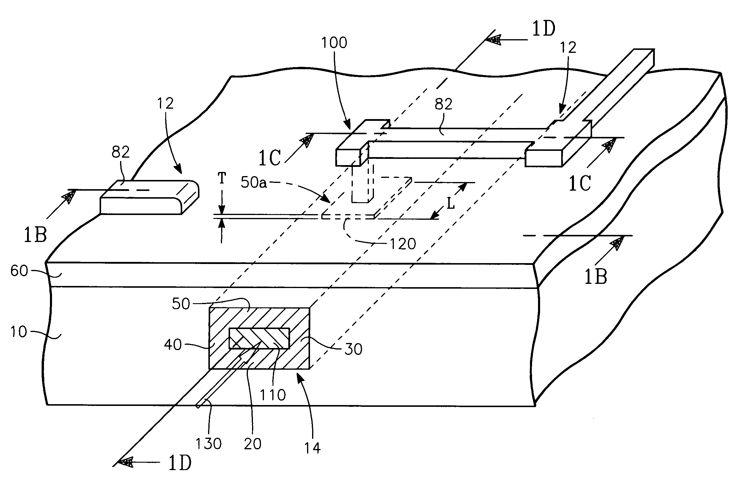
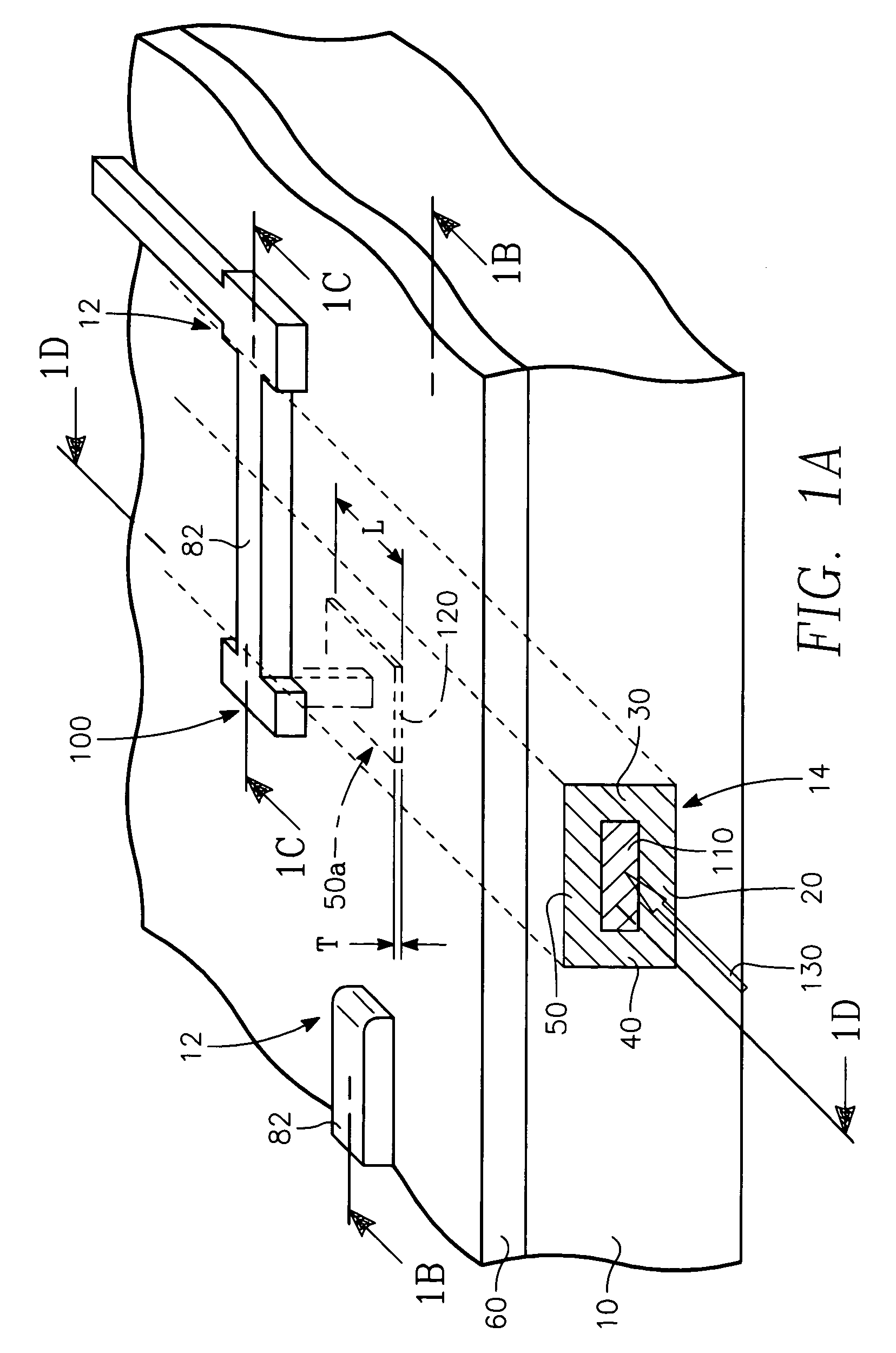
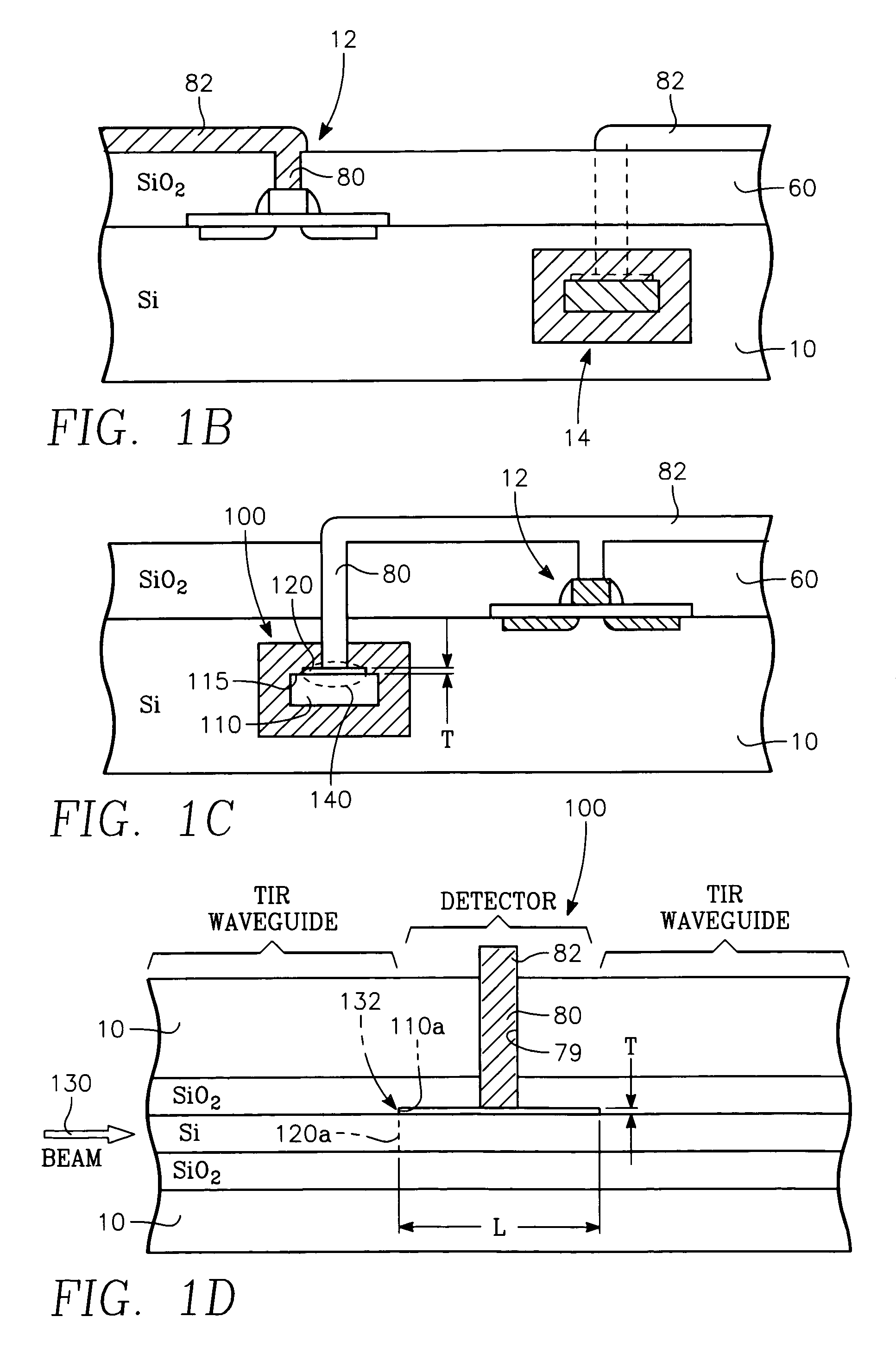
[0025]Referring to FIGS. 1A through FIGS. 1D, a VLSI integrated circuit having a planar structure is formed on a semiconductor substrate 10 including plural transistors 12 formed therein and a buried elongate optical waveguide 14 at least generally beneath the top surface of the semiconductor substrate 10. The semiconductor substrate 10 is typically a silicon wafer, although the substrate 10 may be a silicon layer formed on a semiconductor wafer. The waveguide 14 is a total internal reflection (TIR) waveguide. It consists of an elongate medium or semiconductor layer 110 surrounded on its four sides by a horizontal base layer 20 formed on the substrate 10, a pair of parallel elongate vertical wall layers 30, 40 extending up from the base layer 20, and a ceiling layer 50. The medium, semiconductor layer or core 110 has a different (e.g., higher) index of refraction than the surrounding walls / layers 20, 30, 40, 50. If the elongate core or medium 110 is a semiconductor such as silicon o...


PUM


Abstract

A planar integrated circuit includes a semiconductor substrate having a substrate surface and a trench in the substrate, a waveguide medium in the trench having a top surface and a light propagation axis, the trench having a sufficient depth for the waveguide medium to be at or below said substrate surface, and at least one Schottky barrier electrode formed on the top surface of said waveguide medium and defining a Schottky barrier detector consisting of the electrode and the portion of the waveguide medium underlying the Schottky barrier electrode, at least the underlying portion of the waveguide medium being a semiconductor and defining an electrode-semiconductor interface parallel to the light propagation axis so that light of a predetermined wavelength from said waveguide medium propagates along the interface as a plasmon-polariton wave.

Description

CROSS-REFERENCE TO RELATED APPLICATIONS[0001]This application claims priority of U.S. Provisional Application Ser. No. 60 / 508,421, filed Oct. 3, 2003 entitled A PLANAR INTEGRATED CIRCUIT INCLUDING A PLASMON WAVEGUIDE-FED SCHOTTKY BARRIER DETECTOR AND TRANSISTORS CONNECTED THEREWITH by Gregory Wojcik, et al. and assigned to the present assignee.[0002]This application contains subject matter related to U.S. application Ser. No. 10 / 280,492 filed Oct. 25, 2002 entitled OPTICAL READY WAFERS by Lawrence West et al. and assigned to the present assignee, and U.S. application Ser. No. 10 / 280,505 filed Oct. 25, 2002 entitled OPTICAL READY SUBSTRATES by Claes Bjorkman, et al. and assigned to the present assignee.BACKGROUND[0003]Schottky barrier detectors are used as optical detectors in night vision applications, for example, in which photons in the far infrared range, typically in the 10 micron wavelength region, are detected. Typically, a semiconductor such as silicon is employed with an ove...

Claims


Application Information

Patent Timeline
Patent Type & Authority Patents(United States)
IPC IPC(8): H01L31/00G02B6/12G02B6/122G02B6/42H01L31/0232H01L31/062H01L31/108H01L31/113H01P1/10H01P1/15H01P5/12
CPCB82Y20/00G02B6/12004G02B6/1226H01P1/15H01L31/0232H01L31/108G02B6/42H01L31/02327
Inventor WOJCIK, GREGORY L.WEST, LAWRENCE C.PEARSALL, THOMAS P.
Owner APPLIED MATERIALS INC
Why Eureka
Try Eureka