Methods for forming cobalt layers including introducing vaporized cobalt precursors and methods for manufacturing semiconductor devices using the same

a cobalt layer and cobalt technology, applied in the direction of basic electric elements, electrical equipment, semiconductor devices, etc., can solve the problems of difficult operation of semiconductor devices at a high speed, unsuitable characteristics of semiconductor devices, and increase in power consumption, so as to improve the step coverage

Inactive Publication Date: 2007-02-06
SAMSUNG ELECTRONICS CO LTD
View PDF7 Cites 19 Cited by
  • Summary
  • Abstract
  • Description
  • Claims
  • Application Information

AI Technical Summary

Benefits of technology

[0011]Embodiments of the present invention provide methods for forming cobalt silicide layers capable of having improved step coverage and / or suppressing the formation of an oxide layer at an interface between a silicon substrate and the cobalt silicide layer to provide a desired cobalt silicide layer.

Problems solved by technology

However, when semiconductor devices become highly integrated, the semiconductor devices may have unsuitable characteristics.
As a result, it can be difficult to operate the semiconductor device at a high speed and power consumption can increase.
Further, the cobalt silicide layer formed by silicidating the cobalt layer can possess a low resistance.
The cobalt silicide layer formed by the PVD process, however, has relatively poor step coverage in view of the process characteristics.
Thus, uniformly forming a cobalt layer on a minute and irregular pattern may be problematic.
Since the cobalt layer may typically be formed on the minute and irregular pattern and an inner wall of a contact hole, the PVD process may be less effective for forming the desired cobalt layer.
Moreover, when the cobalt layer has an irregular thickness, the cobalt silicide layer formed from the cobalt layer may also have an irregular thickness so that semiconductor devices on the substrate have various operation characteristics, which can negatively affect reliability of the semiconductor device.
The cobalt layer having an increased quantity of impurities may possess a relatively high resistance so that the CVD process and the ALD process, in addition to the PVD process, may be less effective for forming the desired cobalt layer.

Method used


Image

  • Methods for forming cobalt layers including introducing vaporized cobalt precursors and methods for manufacturing semiconductor devices using the same
  • Methods for forming cobalt layers including introducing vaporized cobalt precursors and methods for manufacturing semiconductor devices using the same
  • Methods for forming cobalt layers including introducing vaporized cobalt precursors and methods for manufacturing semiconductor devices using the same

Examples


example 1

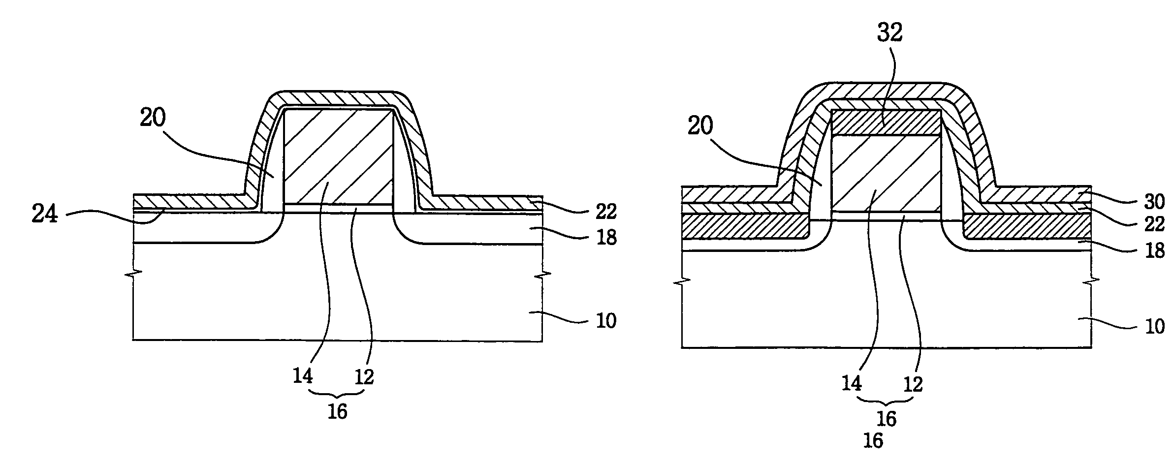
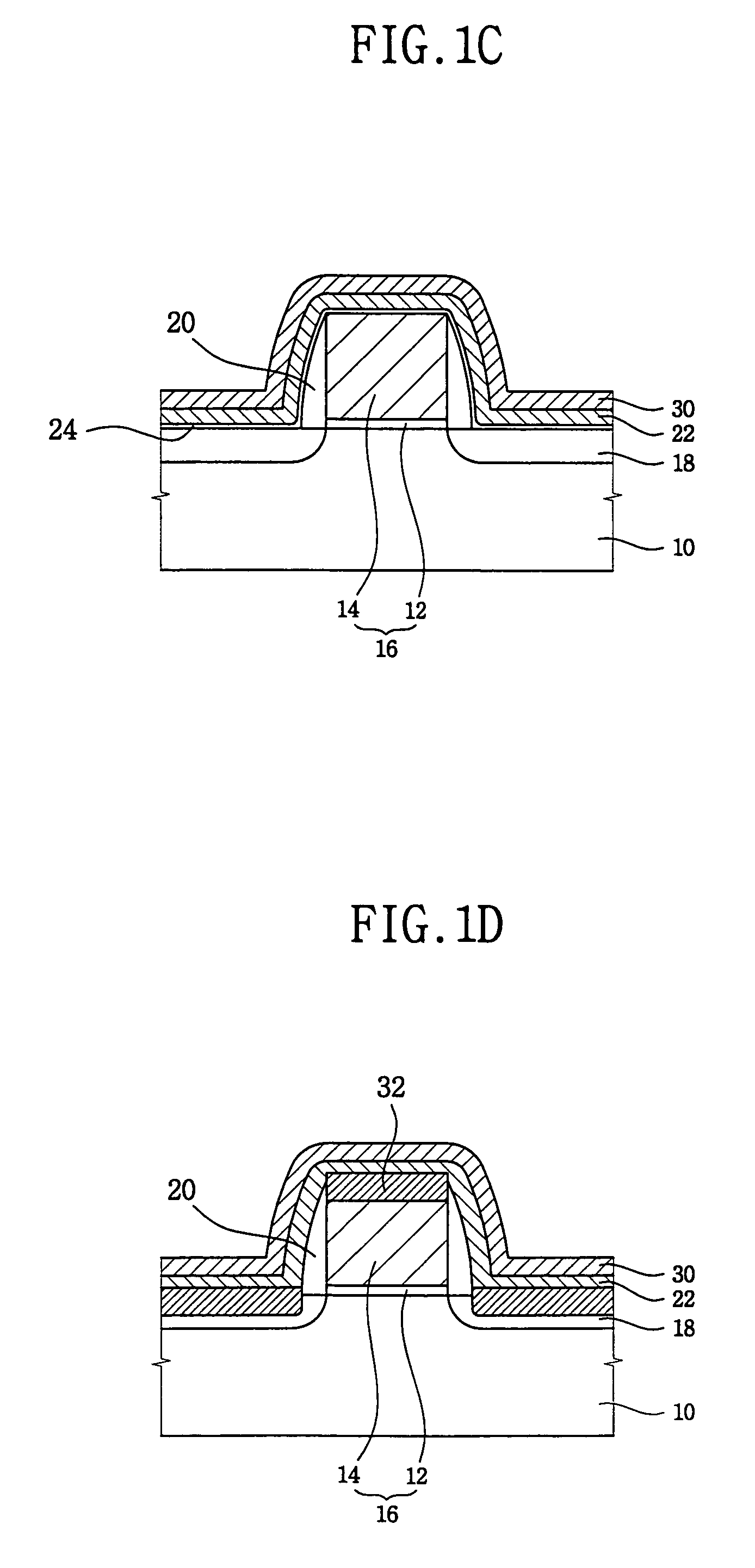
[0045]FIGS. 1A to 1F present cross-sectional views illustrating methods for forming cobalt silicide layers and semiconductor devices including the cobalt silicide layers provided herein.

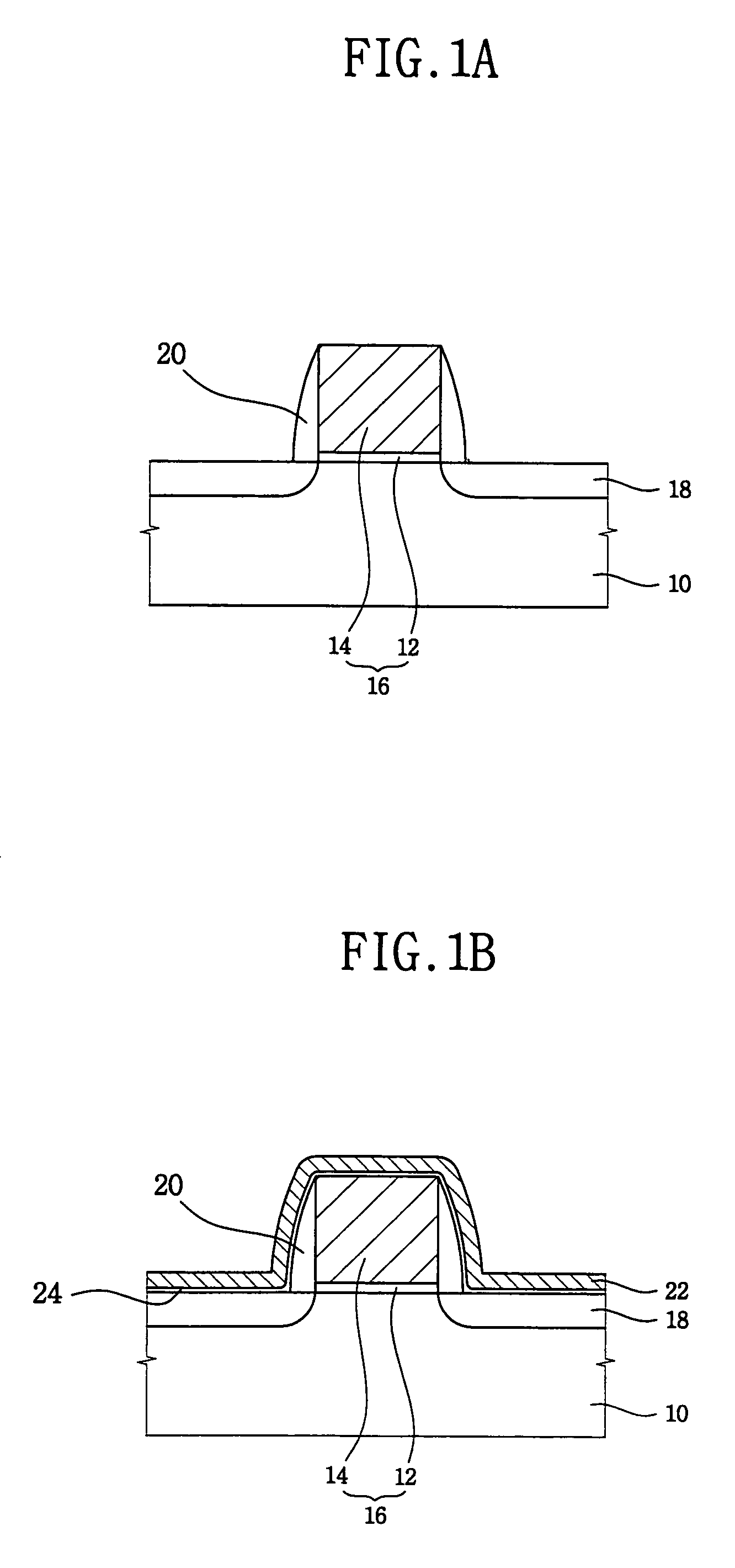
[0046]Referring to FIG. 1A, a silicon substrate 10 was defined into a field region and an active region by an isolation process. A silicon oxide layer having a thickness of about 15 Å was formed on the silicon substrate 10. A polysilicon layer was then formed on the silicon oxide layer. The polysilicon layer and the silicon oxide layer were patterned to form a gate structure 16 including a polysilicon layer pattern 14 and a gate oxide layer pattern 12.

[0047]Impurities were implanted into surface portions of the silicon substrate 10 exposed by the gate structure 16 to form source / drain regions 18. A silicon nitride spacer 20 was formed on a sidewall of the gate structure 16.

[0048]Referring to FIG. 1B, the silicon substrate 10 was wet-cleaned to remove a native oxide layer and particles formed on the s...

example 2

[0062]In further methods of forming a cobalt silicide layer, a gate structure including a gate insulation layer pattern and a polysilicon layer pattern was formed on a silicon substrate. Source / drain regions were formed at surface portions of the silicon substrate at both sides of the gate structure. A silicon nitride spacer was formed on a sidewall of the gate structure.

[0063]A cobalt layer was formed on the silicon substrate and the gate structure. A cobalt precursor was vaporized and introduced onto the silicon substrate. The vaporized cobalt precursor was physisorbed and chemisorbed on the silicon substrate. A purging gas was then introduced onto the silicon substrate. The physisorbed portion was separated from the silicon substrate to leave mostly or only a cobalt atomic layer on the silicon substrate. These processes were repeatedly carried out to form the cobalt layer having a desired thickness.

example 3

[0064]FIGS. 2A to 2E present cross-sectional views illustrating a method for forming a cobalt silicide layer in a contact hole.

[0065]Referring to FIG. 2A, a polysilicon layer 102 was formed on a silicon substrate 100. An insulating interlayer 104 was formed on the polysilicon layer 102. The insulating interlayer 104 was partially etched to form a contact hole 106 exposing the polysilicon layer 104. The contact hole 106 was then cleaned using plasma.

[0066]Referring to FIG. 2B, a cobalt layer 108 was formed on the insulating interlayer 104, and a side face and a bottom face of the contact hole 106. The cobalt layer 108 can be formed as described in the present examples. A native oxide layer 110 was formed on the polysilicon layer 102 exposed through the contact hole 106 in the process for forming the cobalt layer 108.

[0067]Referring to FIG. 2C, a titanium layer 112 having a thickness of at least about 5 Å was formed on the cobalt layer 108. The titanium layer 110 can be formed by a CV...


PUM

PropertyMeasurementUnit
temperatureaaaaaaaaaa

Abstract

The present invention provides methods for forming cobalt silicide layers, including introducing a vaporized cobalt precursor onto a silicon substrate to form a cobalt layer. The vaporized cobalt precursor has the formula Co2(CO)6(R1—C≡C—R2), wherein R1 is H or CH3, and R2 is H, t-butyl, methyl or ethyl. The silicon substrate is thermally treated so that silicon is reacted with cobalt to form a cobalt silicide layer. Methods for manufacturing semiconductor devices including the cobalt silicide layers described herein and such devices are also provided.

Description

RELATED APPLICATION DATA[0001]This application claims the priority of Korean Patent Application No. 2003-65572, filed on Sep. 22, 2003, the disclosure of which is incorporated herein by reference in its entirety as if set forth fully herein.FIELD OF THE INVENTION[0002]The present invention relates to methods of forming cobalt layers and methods for manufacturing semiconductor devices using the same. More particularly, the present invention relates to methods of forming cobalt layers using vaporized cobalt precursors as a source.BACKGROUND OF THE INVENTION[0003]As an information-oriented society has rapidly developed, semiconductor devices capable of rapidly transmitting data to quickly process massive information may be desired. However, when semiconductor devices become highly integrated, the semiconductor devices may have unsuitable characteristics. For example, the length of a gate electrode and the junction depth of source / drain regions can be reduced. Such scaling down of these...

Claims


Application Information

Patent Timeline
Patent Type & Authority Patents(United States)
IPC IPC(8): H01L21/44H01L21/24H01L21/26H01L21/28H01L21/285H01L21/336H01L21/42H01L21/768
CPCH01L21/28052H01L21/28518H01L29/665H01L21/76889H01L21/28556H01L21/24
Inventor KIM, HYUN-SUCHOI, GIL-HEYUNKANG, SANG-BOMSOHN, WOONG-HEEYUN, JONG-HOMOON, KWANG-JIN
Owner SAMSUNG ELECTRONICS CO LTD
Why Eureka
Try Eureka