

Resolution enhancement for macro wafer inspection
- Summary
- Abstract
- Description
- Claims
- Application Information
AI Technical Summary
Benefits of technology
Problems solved by technology
Method used
Image

Examples
first embodiment
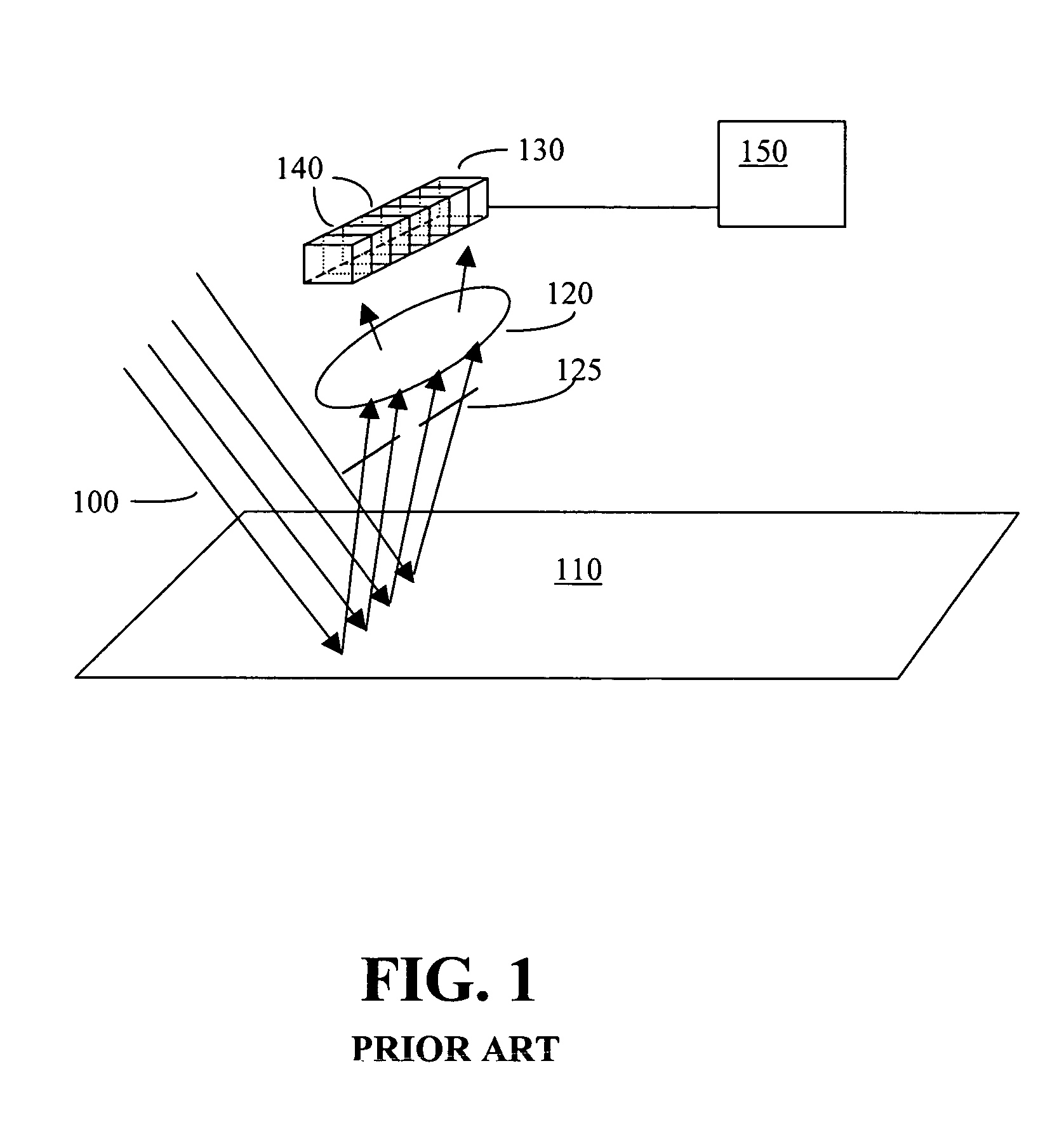
[0024]According to the method of the present invention, the effective pixel resolution is improved by utilizing a sampling phase shift between successive lines of a multi-line sensor array during scanning. Corresponding pixels in successive lines are offset by a portion of a pixel. Although each pixel is still integrating the signal across its full width, the information content of corresponding pixels in each channel is now different. By numerical deconvolution, the sampling can be reconstructed as though the sampling had been done with a single channel containing a larger number of pixels. Discussions of applicable numerical deconvolution techniques are found in:
Lucy, L. B., Astron. Journal 79, pp 745 (1974), Richardson, W. H., J. Opt. Soc. Am., 62, pp 55 (1972), and Digital, mage Processing, Rafel C. Gonzalez and Richard E. Woods, Addison Wesley, 1992, pp 195 ff.
[0025]A preferred method of achieving this phase shift is accomplished with a simple modification to the geometry of th...
second embodiment
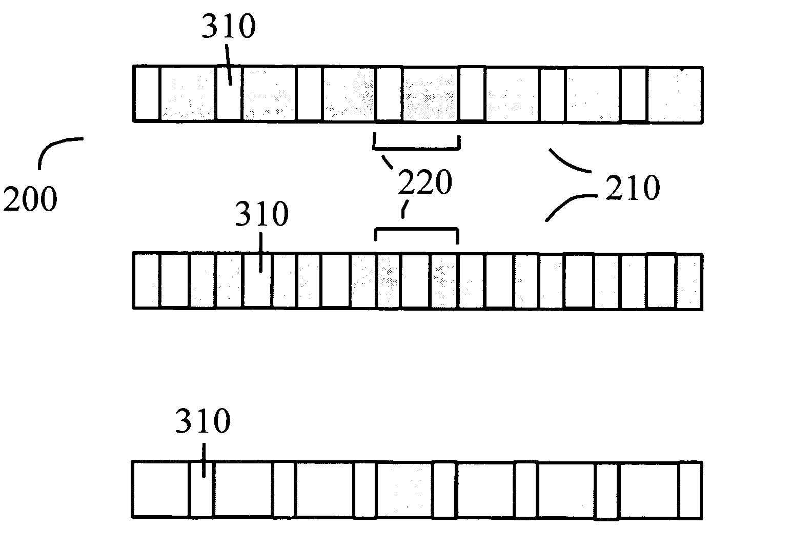
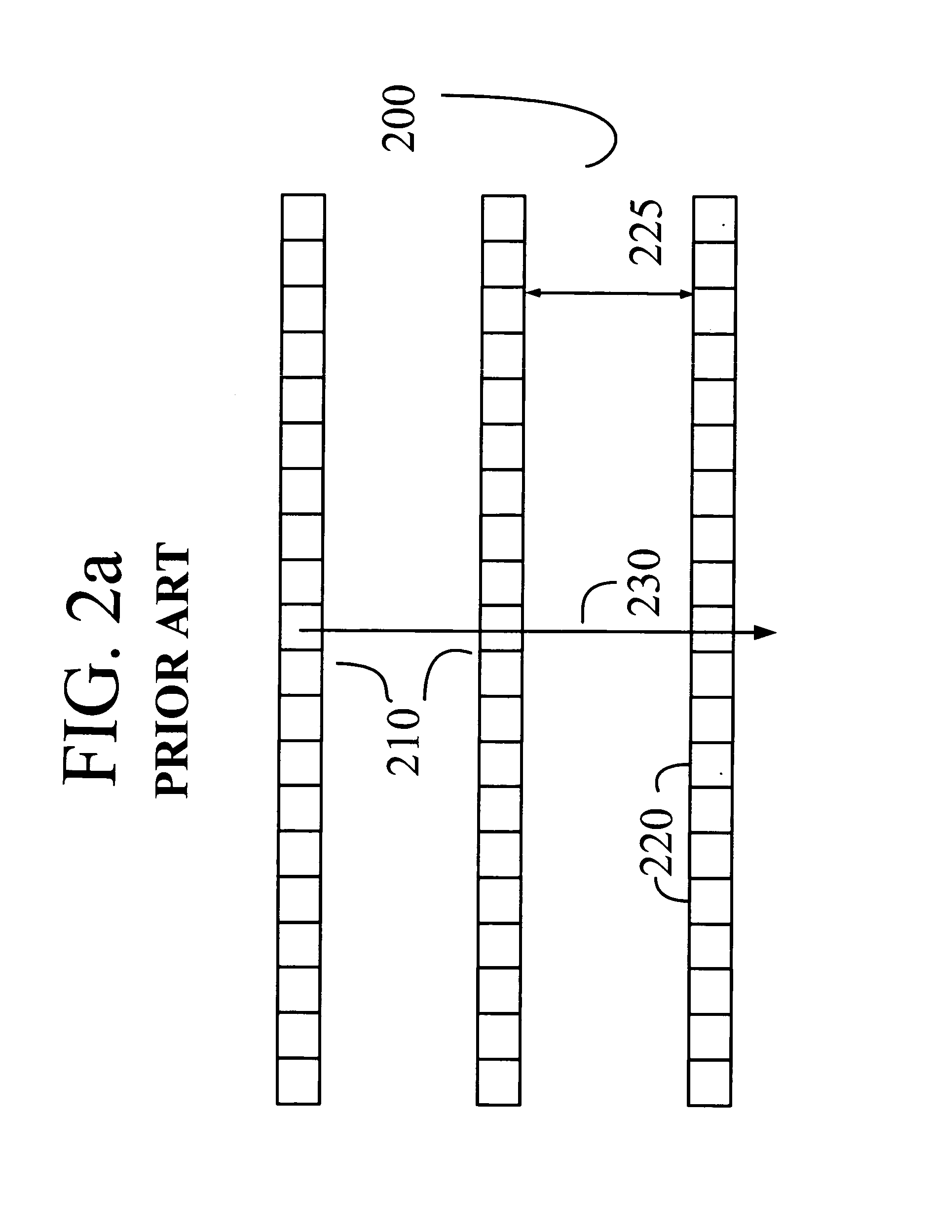
[0028]In the invention, illustrated in FIG. 3, effective pixel density increase is achieved by masking portions of each sensor: the sensor manufacturer deposits an opaque mask over each channel, wherein only a fraction of each pixel is left unmasked (in the example shown, ⅓ of each pixel is left unmasked). The unmasked portion 310 is shifted in each successive channel, such that the sampling is performed at progressively offset locations. Using this method, a true (3× in the illustrated example) effective pixel density increase is achieved, and horizontal resolution is improved, without the necessity of deconvolving overlapping signals. Well capacity remains the same for each sensor and therefore Schott noise is not increased, even though the exposed photosensitive surface area is decreased. However, increased illumination intensity is required, and custom modifications are needed to the sensor array. Resolution in the direction of the scan can be improved by reading more lines with...
PUM
 Abstract
Description
Claims
Application Information