
Manufacturing method and apparatus to avoid prototype-hold in ASIC/SOC manufacturing

a manufacturing method and a technology for asic/soc manufacturing, applied in the field of manufacturing methods and equipment for large-scale integrated circuits, can solve problems such as failures in prototype evaluation, silicon cannot be used for application development, and the production process is suspended, so as to save engineering time and reduce the overall cost involved

Inactive Publication Date: 2007-02-13
ADVANTEST CORP
View PDF17 Cites 15 Cited by
  • Summary
  • Abstract
  • Description
  • Claims
  • Application Information

AI Technical Summary

Benefits of technology

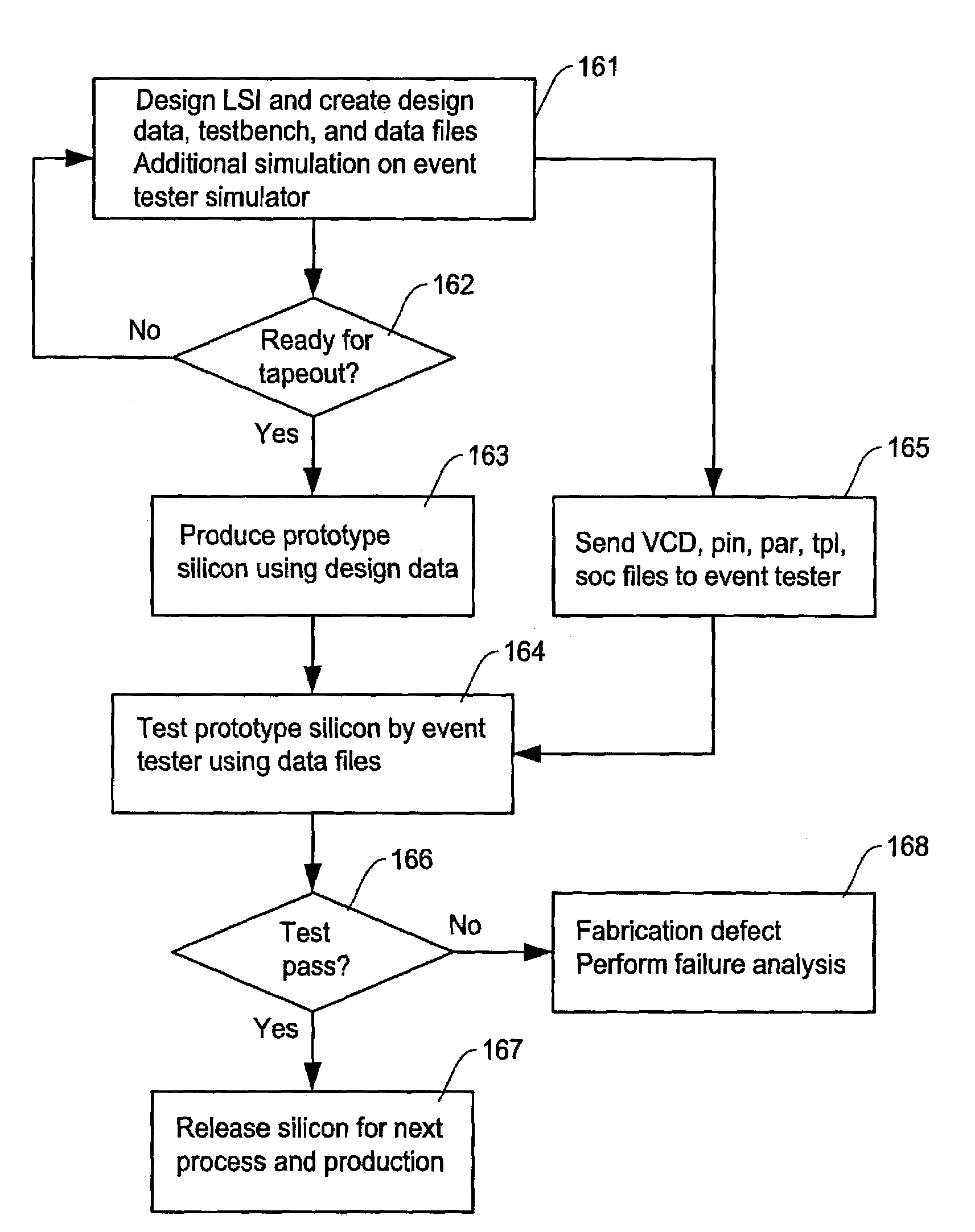
[0007]It is, therefore, an object of the present invention to provide a new semiconductor production method incorporating a new type of semiconductor IC test system which is capable of avoiding the prototype-hold problems interrelating with the design environment and test engineering environment in a seamless fashion.
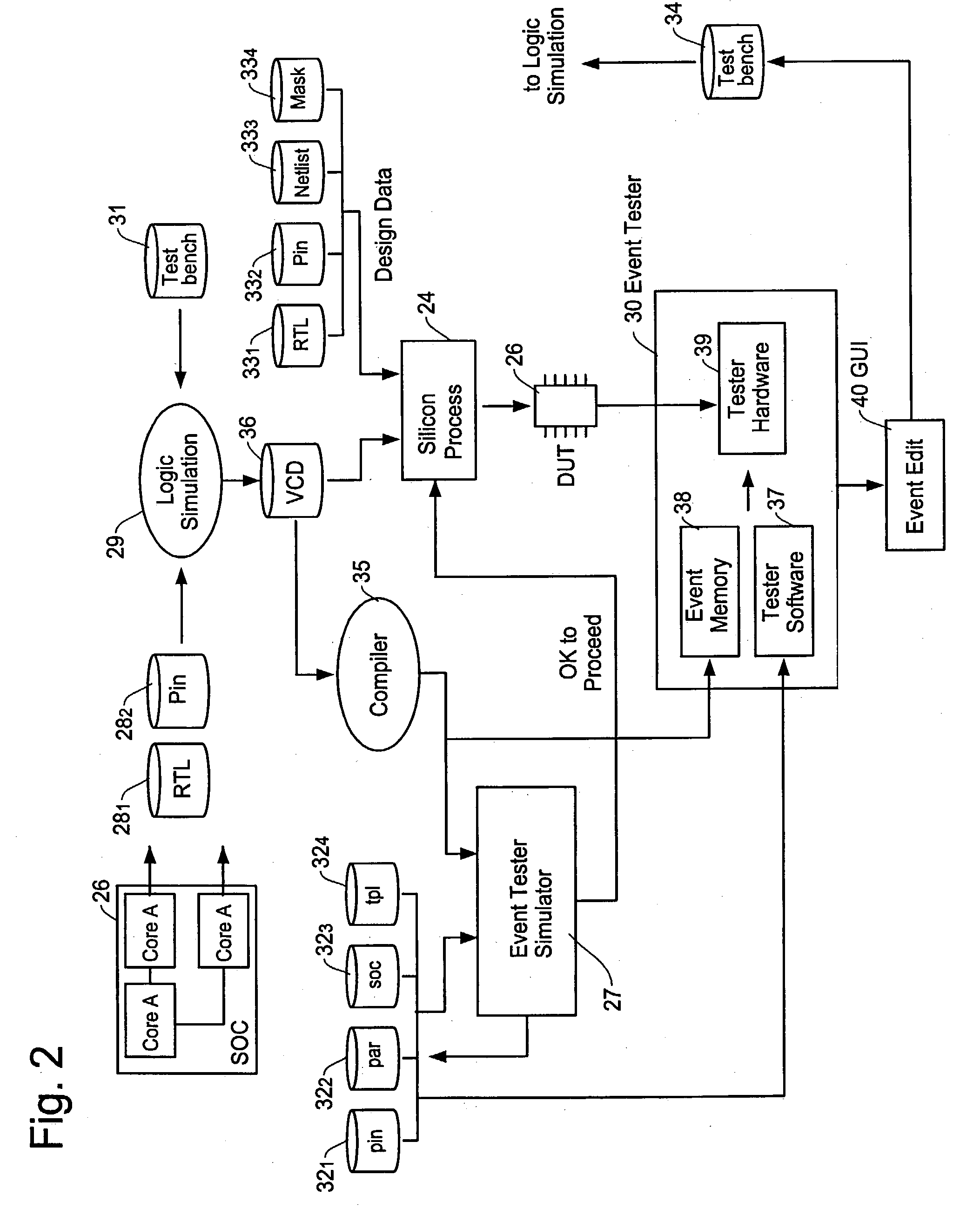
[0009]It is a further object of the present invention to provide a new semiconductor production method incorporating a new semiconductor IC test system (event tester) in a test-engineering environment and an event tester simulator in an EDA environment, thereby eliminating needs of creating test vectors and test programs in the test-engineering environment.
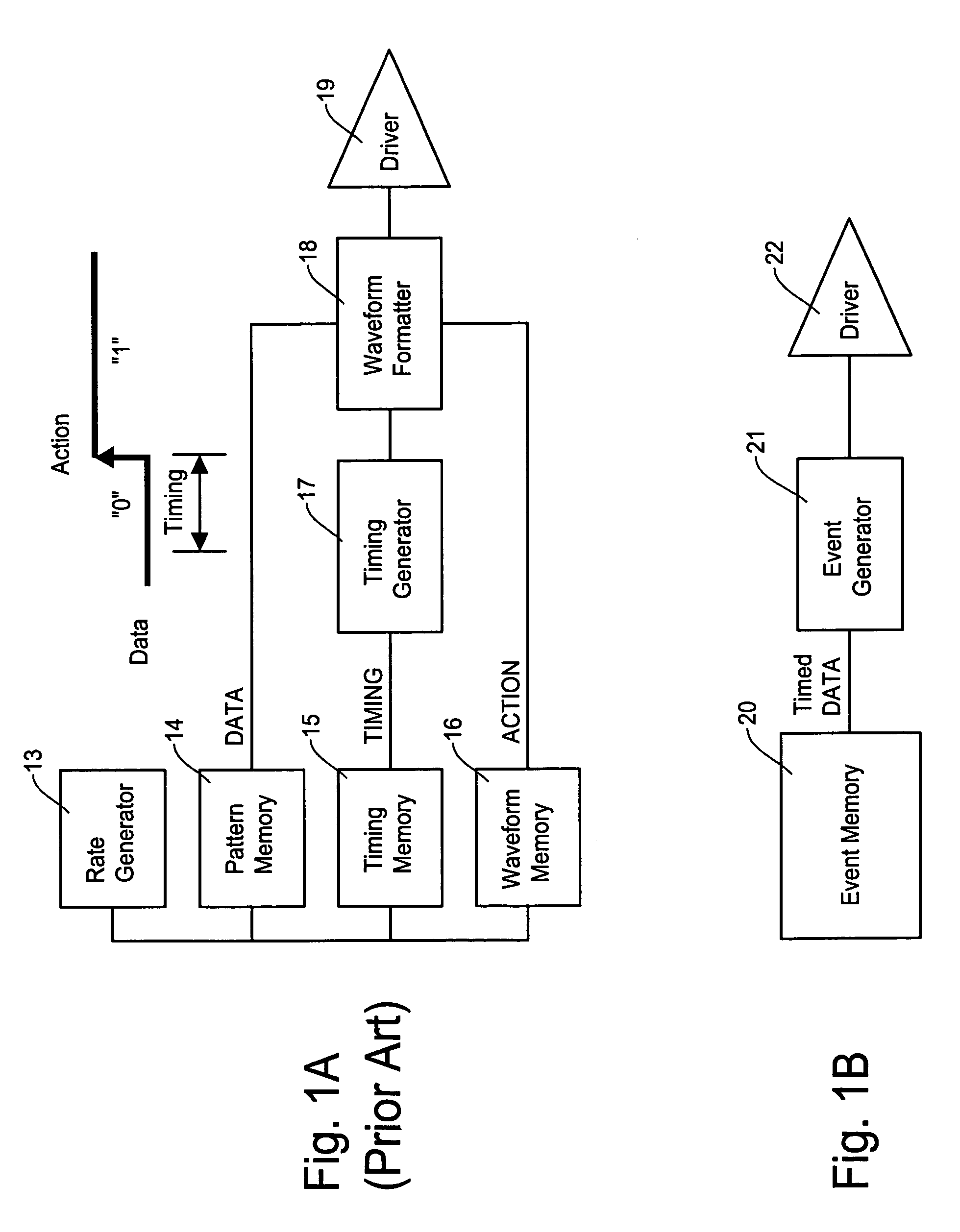
[0011]According to the present invention, the method and architecture of the test system allows testing and debug of ICs without diverting from the environment in which the IC was designed. The traditional IC test systems require conversion of the design simulation data into a cyclized form, such as the WGL or STIL format. The new method and architecture avoids such conversion and uses the design simulation data “as is”. Thus, the method and apparatus of the present invention allow testing in the environment identical to the design simulation environment, which avoids the proto-hold. The new semiconductor production process incorporates the event tester in the test-engineering environment and the event tester simulator in the EDA environment, thereby eliminating needs of creating the test vectors and test programs in the test-engineering environment, which saves engineering time and reduces overall cost involved in the LSI production.

Problems solved by technology

One of the major issues today in manufacturing LSI such as ASIC (application specific integrated circuit) or SOC (system-on-a-chip) is a standstill of a production process in the prototype test.
More than 50% ICs coming out of the prototype fabrication stage fail to pass the test, which results in suspension of the production process to the next stage (ex. application development and mass production).
When the first silicon (prototype LSI) comes out of fabrication, in majority of cases, it shows some failures in the prototype evaluation.
The cause of these failures varies; it can be an error in vector translation (test data conversion), or an error in a test program or even fabrication defects.
In a large number of cases, the cause of failure is not easily identifiable and hence, the silicon (prototype LSI) is put on prototype hold (proto-hold).
Until the cause is identified and rectified, the silicon cannot be used for application development and subsequently it cannot go into volume production.
The primary factor behind this issue is that the design environment is different from the test-engineering environment and therefore, the cause of failure is not easily identified.
Hence, when the first silicon (prototype LSI chip) shows a failure (failing vector in the test vectors), it is quite cumbersome to determine the cause of the failure.
The semiconductor industry involves extremely expensive and large scale production facilities and a production volume of each LSI device is large.
Thus, such a delay caused by the proto-hold is extremely costly for application developers, the design house (ASIC house or design center) as well as for the silicon foundry (semiconductor manufacture).

Method used


Image

  • Manufacturing method and apparatus to avoid prototype-hold in ASIC/SOC manufacturing
  • Manufacturing method and apparatus to avoid prototype-hold in ASIC/SOC manufacturing
  • Manufacturing method and apparatus to avoid prototype-hold in ASIC/SOC manufacturing

Examples


Embodiment Construction

[0024]The present invention is now described in more detail with reference to the accompanying drawings. The present invention proposes a new LSI manufacturing process incorporating an event based test system (event tester) for the LSI manufacturing in which there is no proto-hold. This method is based upon a new technology, a new equipment and fundamental changes in the existing process. The concept and architecture of new equipment, semiconductor manufacturing process based upon it and specific data format used are described in this application.

[0025]In the production process of the present invention, rather than the conventional cycle based test system (cyclized tester), an event based test system (event tester) is used to test the prototype LSI chip such as an ASIC or SOC. In the design environment (design house), a design engineer creates various files for implementing the test on the chip by the event tester. Such files include test pattern data, test parameter data, tester ch...


PUM


Abstract

A manufacturing process for LSIs uses an event tester simulator and an event tester to avoid prototype hold. In the LSI manufacturing method an LSI is designed under an EDA (electronic design automation) environment to produce design data of a designed LSI, and logic simulation is performed on a device model of the LSI design in the EDA environment with use of a testbench and producing a test vector file of an event format as a result of the logic simulation. Then, simulation data files are verified with use of the design data and the testbench by operating an event tester simulator, and a prototype LSI is produced through a fabrication provider by using the design data. The prototype LSI is tested by an event tester by using the test vector file and the simulation data files and test results is feedbacked to the EDA environment or the fabrication provider.

Description

[0001]This application claims the benefit of U.S. Provisional Application Ser. No. 60 / 371,808 filed Apr. 11, 2002.FIELD OF THE INVENTION[0002]This invention relates to a manufacturing method and apparatus for large scale integrated circuits (LSI), and more particularly, to a manufacturing method for LSIs using an event based IC test system in which test data is utilized in an event form which enables a direct use of design simulation data produced in an electronic design automation (EDA) environment, thereby avoiding prototype-hold in the LSI manufacturing.BACKGROUND OF THE INVENTION[0003]This application describes a modified industrial process for LSI manufacturing. One of the major issues today in manufacturing LSI such as ASIC (application specific integrated circuit) or SOC (system-on-a-chip) is a standstill of a production process in the prototype test. More than 50% ICs coming out of the prototype fabrication stage fail to pass the test, which results in suspension of the prod...

Claims


Application Information

Patent Timeline
Patent Type & Authority Patents(United States)
IPC IPC(8): G06F17/50G01R31/28H01L21/822G01R31/317G01R31/3183G01R31/319G06F19/00H01L21/02H01L21/82H01L27/04H01L27/118
CPCG01R31/318314G06F17/5022G01R31/31704H01L27/118G01R31/31917G06F30/33H01L21/00
Inventor RAJSUMAN, ROCHITYAMOTO, HIROAKI
Owner ADVANTEST CORP
Learn More