Low-jitter adjustable level shifter with native devices and kicker

a level shifter and native device technology, applied in logic circuits, logic circuit coupling/interface arrangements, pulse techniques, etc., can solve the problems of slow switching speed, low jitter performance of conventional level shifter circuits, and inability to adjust, etc., to achieve low jitter and high switching speed

Inactive Publication Date: 2007-02-20
ALTERA CORP
View PDF10 Cites 34 Cited by
  • Summary
  • Abstract
  • Description
  • Claims
  • Application Information

AI Technical Summary

Benefits of technology

[0010]A delay circuit is connected between the output of the first inverter and the gate of a first of the native devices. The delay circuit may include two cascaded inverters. The delay circuit helps ensure that the shape of the output data pulses is the same as the shape of the input data pulses provided to the level shifter.
[0011]A thick-oxide n-channel metal-oxide-semiconductor kicker transistor is connected in parallel with one of the p-channel metal-oxide-semiconductor transistors to help the level shifter pull up the output terminal during low to high data transitions. The kicker transistor gate is connected to the gate of one of the native transistors and the gate of one of the thin-oxide transistors.
[0012]The level shifter exhibits low jitter and high switching speeds.

Problems solved by technology

Conventional level shifter circuits often exhibit suboptimal jitter performance and slow switching speeds or are not adjustable.

Method used


Image

  • Low-jitter adjustable level shifter with native devices and kicker
  • Low-jitter adjustable level shifter with native devices and kicker
  • Low-jitter adjustable level shifter with native devices and kicker

Examples


Embodiment Construction

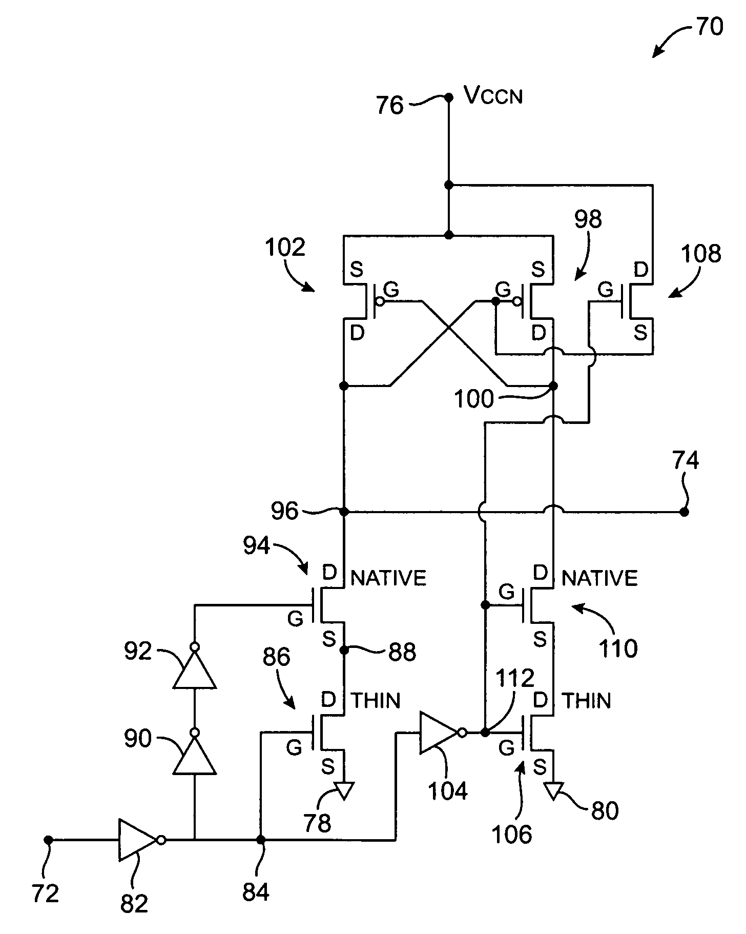
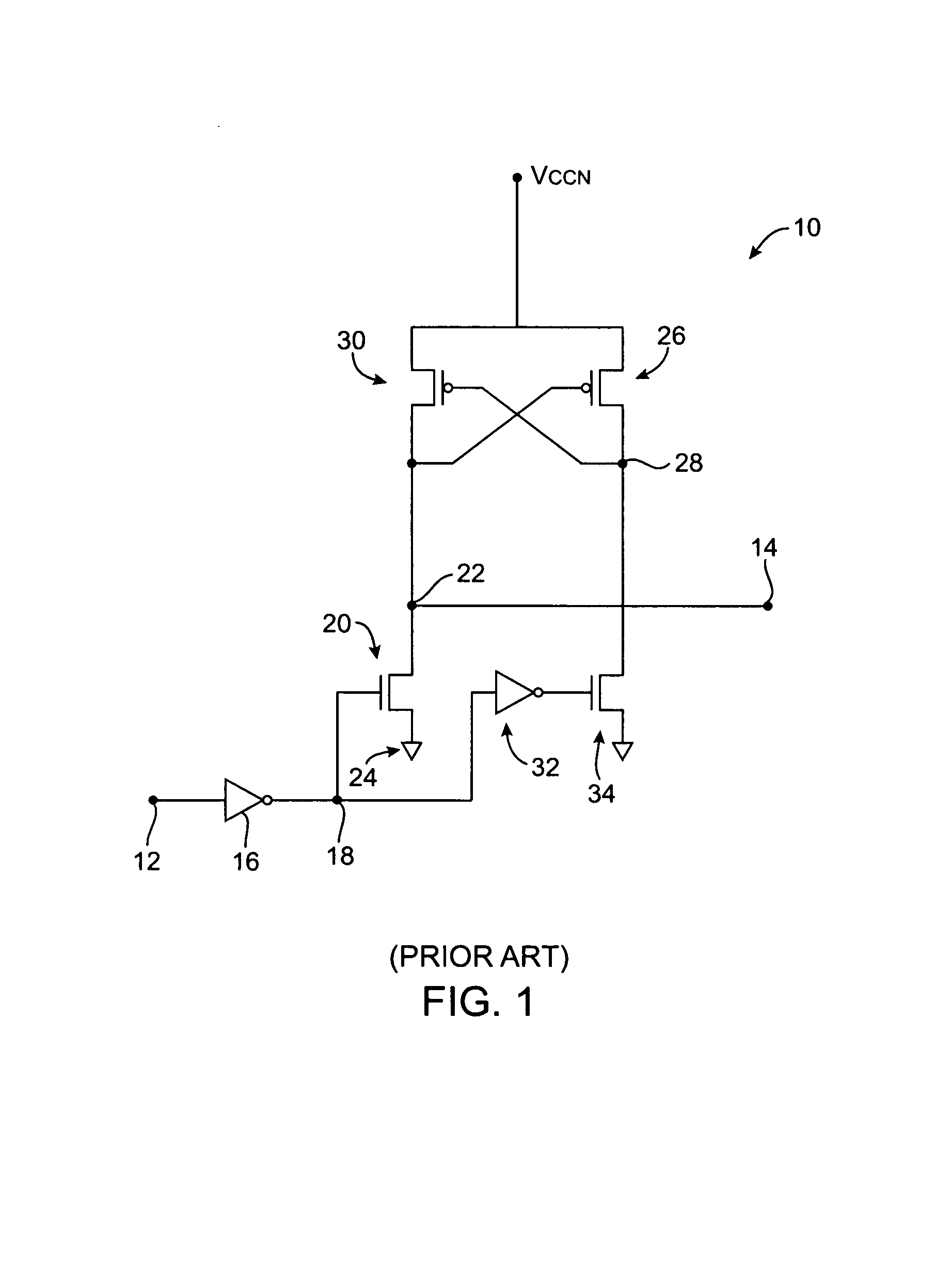
[0023]The present invention relates to integrated circuit level shifting circuitry for converting digital data signals with one voltage range (e.g. 0–1.2 volts) to digital data signals with another voltage range (e.g., 0–2.5 volts). The present invention also relates to methods for adjusting and operating such level shifting circuitry.

[0024]Digital integrated circuits typically handle data internally in the form of single-ended signals. Single-ended signals are referenced to ground. If a single-ended signal has a high voltage (e.g., a voltage near a positive power supply voltage), that signal is said to be “high” (i.e., it represents a logic “1”). If a single-ended signal has a low voltage (e.g., a voltage near ground), that signal is said to be “low” (i.e., it represents a logic “0”). The voltage swing of the digital signals (i.e., the difference between the high voltage level and the ground voltage) may be, for example, 1.2 volts.

[0025]A voltage swing of 1.2 volts may be suitable ...


PUM


Abstract

An adjustable level shifter with native and kicker transistors is provided. The level shifter provides high switching speeds, adjustable output voltage levels, and low jitter. The level shifter has first and second thick-oxide p-channel metal-oxide-semiconductor (PMOS) transistors, first and second thick-oxide native n-channel metal-oxide-semiconductor (NMOS) transistors, and first and second thin-oxide NMOS transistors. The first PMOS transistor, first native transistor, and first NMOS transistor are connected in series and the second PMOS transistor, second native transistor, and second NMOS transistor are connected in series. An input data signal and an inverted version of the input data signal drive the gates of the thin-oxide NMOS transistors. A node located between the first PMOS transistor and first native transistor is connected to an output data terminal. The kicker transistor is connected in parallel with the first PMOS transistor.

Description

BACKGROUND OF THE INVENTION[0001]This invention relates to level shifters, and more particularly, to adjustable level shifters with low jitter.[0002]Level shifting circuits are used to change the voltage range of digital signals. Digital data input signals are received at a level shifter input and corresponding level-shifted digital data output signals are provided at a level shifter output. A level shifter may, for example, convert 1.5 volt input signals to 3.3 volt output signals. Because the maximum voltage of the output data (3.3 volts) is different from the maximum voltage of the input data (1.5 volts), the signal level is said to be “shifted.”[0003]Adjustable level shifter circuits are used in environments in which it is desired to provide user control over the output voltage level. In a typical adjustable level shifter arrangement, the level shifter is located on an integrated circuit and has a power supply terminal that is connected to one of the integrated circuit's input p...

Claims


Application Information

Patent Timeline
Patent Type & Authority Patents(United States)
IPC IPC(8): H03K19/0175
CPCH03K3/356113H03K3/013
Inventor SIA, KET CHIEWWONG, CHOONG KITOOI, BOON HAWTEE, KOK SIONG
Owner ALTERA CORP
Why Eureka
Try Eureka