

Semiconductor memory device with column selecting switches in hierarchical structure
a memory device and switch technology, applied in the field of semiconductor memory devices, can solve the problems of increasing the burden on the column selecting line (ys), posing a large burden, and so as to achieve the effect of reducing the signal delay
- Summary
- Abstract
- Description
- Claims
- Application Information
AI Technical Summary
Benefits of technology
Problems solved by technology
Method used
Image

Examples
1st embodiment
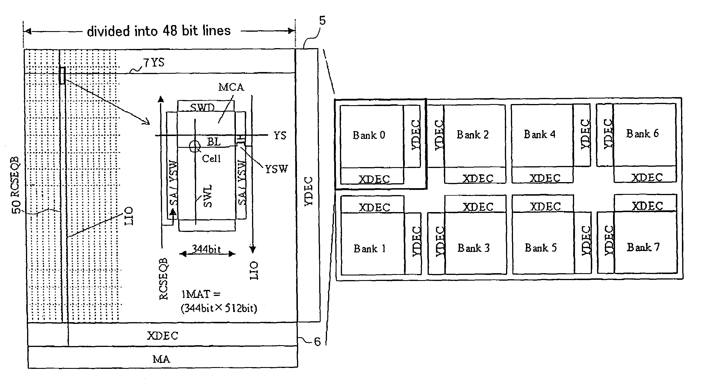
[0041]FIG. 3 shows in block form a general arrangement of a memory cell array of a semiconductor memory device according to a first embodiment of the present invention. The semiconductor memory device according to the first embodiment of the present invention has peripheral circuits of the memory cell array which are identical to those shown in FIG. 1.
[0042]FIG. 3 shows a 1-Gbit DRAM chip layout of the semiconductor memory device according to the first embodiment of the present invention. In FIG. 3, the memory cell array comprises eight banks each of 128 Mbits, with a row decoder (XDEC) and a column decoder (YDEC) disposed in each of the banks. Each of the banks is divided into memory cell arrays represented by 16 mats×48 rows and has 48 divided bit lines arranged in the X direction. Each of the mats comprises a memory cell array of 344 bits×512 bits surrounded by SA / YSW areas and SWD areas.
[0043]FIG. 4 shows an internal structure (YSW hierarchical structure) of the memory cell arra...
2nd embodiment
[0065]A semiconductor memory device according to a second embodiment of the present invention will be described below. The semiconductor memory device according to the second embodiment is basically of the same arrangement as the semiconductor memory device according to the first embodiment. However, the semiconductor memory device according to the second embodiment has another YS hierarchical structure. FIG. 7 shows a structure of a memory cell array of the semiconductor memory device according to the second embodiment. Those parts shown in FIG. 7 which are identical to those shown in FIG. 4 are denoted by identical reference characters, and will not be described in detail below.
[0066]The memory cell array of the semiconductor memory device according to the second embodiment differs from the circuit arrangement shown in FIG. 4 in that global column selecting switch (GYSW) 10 in the form of a PMOS transistor is replaced with global column selecting switch (GYSW) 70 in the form of an...
PUM
 Abstract
Description
Claims
Application Information