Semiconductor memory having charge trapping memory cells and fabrication method

a technology of memory cells and semiconductors, applied in semiconductor devices, digital storage, instruments, etc., can solve the problems of inability to quickly access the memory contents, difficulty in various difficulties, and memory cells that cannot be miniaturized more extensively, so as to reduce the electrical bulk resistance

Inactive Publication Date: 2007-02-27
POLARIS INNOVATIONS LTD
View PDF20 Cites 6 Cited by
  • Summary
  • Abstract
  • Description
  • Claims
  • Application Information

AI Technical Summary

Benefits of technology

[0013]In accordance with a consecutive numbering of the memory transistors along a respective word line, the cross-connections electrically conductively connect, on one side of the word line, in each case a source / drain region of an even-numbered memory transistor to a source / drain region of the subsequent odd-numbered memory transistor in the numbering and, on the opposite side of this word line, in each case a source / drain region of an odd-numbered memory transistor to a source / drain region of the subsequent even-numbered memory transistor in the numbering. The word lines can be contact-connected between the bit lines with word line straps that reduce the electrical bulk resistance.

Problems solved by technology

WO 99 / 60631) having planar MOS transistors and an oxide-nitride-oxide storage layer sequence as gate dielectric require voltages of 4 to 5 volts for programming and erasing, which may be regarded as a disadvantage.
Moreover, the memory cells can only be miniaturized more extensively if they are not arranged in one plane one beside the other but rather at the walls of trenches, which are etched out at the top side of a semiconductor body.
This results in various difficulties.
The word lines have a small cross section, so that fast access to the memory contents is not possible owing to the low electrical conductivity caused as a result of the small cross section.
Since the isolation between adjacent channel regions is preferably effected by a channel stop implantation, dopants diffusing into the channel region can bring about a non-uniform current distribution in the channel together with a significant occurrence of the narrow width effect.

Method used


Image

  • Semiconductor memory having charge trapping memory cells and fabrication method
  • Semiconductor memory having charge trapping memory cells and fabrication method
  • Semiconductor memory having charge trapping memory cells and fabrication method

Examples


Embodiment Construction

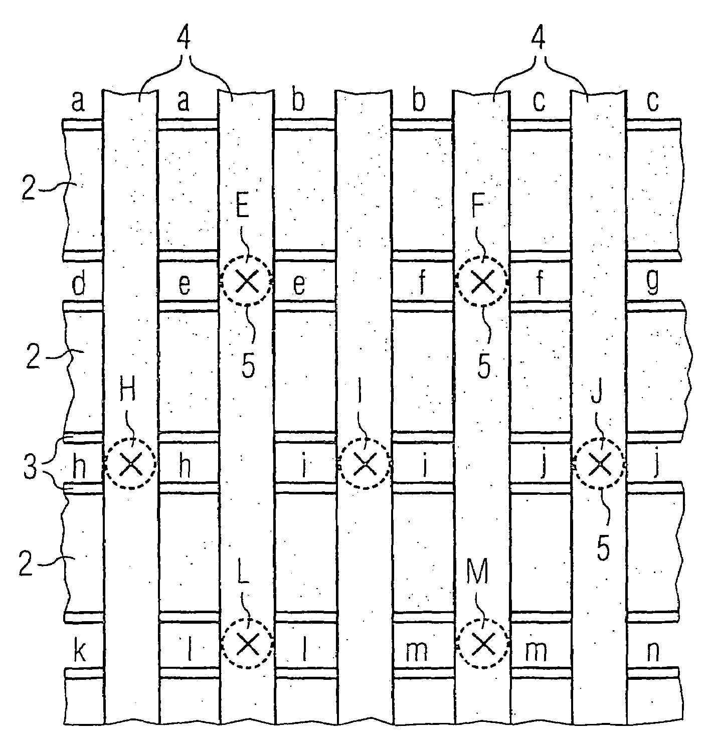
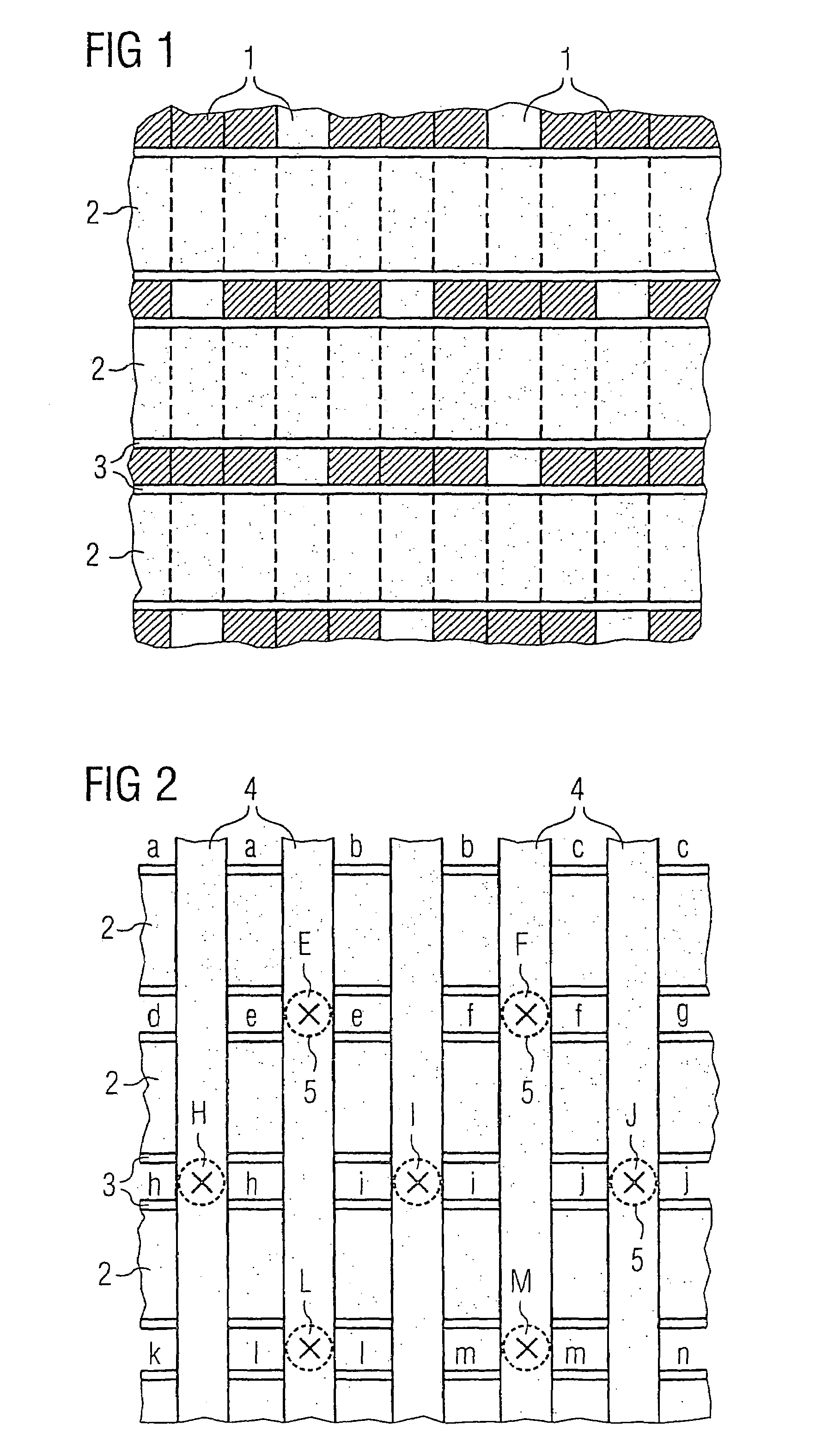
[0058]FIG. 1 shows a plan view of a scheme revealing the positions of the STI isolations 1, word lines 2 with lateral spacers 3 and the regions that are to be electrically conductively connected to one another. The STI isolations (shallow trench isolation) are isolation trenches that are arranged parallel at a distance from one another and between which there are in each case channel regions of the transistors that run parallel to the isolation trenches below each word line 2. The word lines, therefore, run over the channel regions arranged transversely with respect to the longitudinal direction of the word line. The source / drain regions of the transistors are in each case present in a manner laterally adjoining the word lines. The source / drain regions are electrically conductively connected to one another in the regions that are in each case identified in hatched fashion in FIG. 1, a short piece of the relevant isolation trench being bridged in each case.

[0059]FIG. 2 illustrates a ...


PUM


Abstract

In the case of this semiconductor memory having NROM cells, the channel regions of the memory transistors in each case run transversely with respect to the relevant word line, the bit lines are arranged on the top side of the word lines and in a manner electrically insulated from the latter, and electrically conductive cross-connections are present, which are arranged in sections in interspaces between the word lines and in a manner electrically insulated from the latter and are connected to the bit lines in each case in next but one sequence.

Description

[0001]This application is a continuation of International Application No. PCT / EP2003 / 014172, filed Dec. 12, 2003, which designated the United States and was published in English, and which is based on German Application No. 102 58 194.0, filed Dec. 12, 2002, both of which applications are incorporated herein by reference.TECHNICAL FIELD[0002]The present invention relates generally to semiconductor devices and methods, and more particularly to a semiconductor memory having charge-trapping memory cells and fabrication method.BACKGROUND[0003]Memory cell arrays comprising charge-trapping memory cells having memory transistors that can be programmed by channel hot electrons (CHE) and can be erased by hot holes, for example, in particular comprising planar SONOS memory cells or NROM memory cells (U.S. Pat. No. 5,768,192, U.S. Pat. No. 6,011,725 and International Patent No. WO 99 / 60631) having planar MOS transistors and an oxide-nitride-oxide storage layer sequence as gate dielectric requi...

Claims


Application Information

Patent Timeline
Patent Type & Authority Patents(United States)
IPC IPC(8): G11C5/06H01L21/8246H01L27/115
CPCH01L27/11568H01L27/115H10B69/00H10B43/30H01L29/42324
Inventor BOLLU, MICHAELKOHLHASE, ARMINLUDWIG, CHRISTOPHPALM, HERBERTWILLER, JOSEF
Owner POLARIS INNOVATIONS LTD
Why Eureka
Try Eureka