Semiconductor memory having a dummy signal line connected to dummy memory cell

a technology of semiconductor memory and signal line, which is applied in the direction of digital storage, electronic circuit testing, instruments, etc., can solve the problems of data lost in the real memory cell, and achieve the effect of preventing the increase of the chip size of the semiconductor memory, facilitating the operation, and reducing the amount of leakag

Inactive Publication Date: 2007-02-27
SOCIONEXT INC
View PDF5 Cites 8 Cited by
  • Summary
  • Abstract
  • Description
  • Claims
  • Application Information

AI Technical Summary

Benefits of technology

[0009]In a semiconductor memory according to one aspect of the present invention, real signal lines are connected respectively to a plurality of real memory cell rows each of which is formed of real memory cells arranged in one direction. The first dummy signal line is wired along the real signal lines on the outside of a region in which the real memory cells are arranged. The first dummy memory cells are connected to the first dummy signal line, so that a predetermined logical level can be written onto the first dummy memory cells during a test mode. The first dummy memory cells have the same shape and characteristics as those of the real memory cells and are arranged adjacent to the real memory cells. A voltage setting circuit sets the first dummy signal line to the first voltage in order to keep the first dummy memory cell in a non-written state during a normal operation mode. Moreover, the voltage setting circuit sets the first dummy signal line to the second voltage in order to write test data onto the first dummy memory cell during the test mode. By writing data of a logic that is opposite to that of the test data onto the real memory cell adjacent to the first dummy memory cell by means of an operation control circuit, it is possible to check a leak failure that may occur between the real memory cell and the first dummy memory cell that are adjacent to each other. In other words, it is possible to detect a failure of the outermost real memory cell, which cannot be detected by the conventional technique. Thus, it is possible to remove a semiconductor memory having the aforementioned leak failure as a defective product in the first half of a test process consisting of a plurality of tests, which can eliminate the necessity to test such a defective product in the latter half of the test process and thereby reduce a test cost. Moreover, it is also possible to prevent the semiconductor memory having the leak failure from being shipped to the market.
[0016]In a preferred example of the semiconductor memory according to one aspect of the present invention, the real memory cells and first dummy memory cells each includes a memory element and a transfer switch connected to the memory element. The real signal line is a real bit line connected to the transfer switches of the real memory cells. The first dummy signal line is a dummy bit line connected to the transfer switches of the first dummy memory cells. The first voltage is a precharge voltage that is a reset voltage for the real bit lines and the dummy bit line. The second voltage is a voltage for writing a high logical level onto the real memory cell and the first dummy memory cell. Thus, during the test mode, the aforementioned leak failure can be detected by setting the dummy bit line to the second voltage, writing test data onto the first dummy memory cell, and writing data having a logic opposite to that of the test data onto the real memory cell adjacent to the first dummy memory cell by means of the operation control circuit. During the normal operation mode, the dummy bit line is set to the precharge voltage. Therefore, it is possible to prevent strong stress from being applied to between the real memory cell and the first dummy memory cell that are adjacent to each other.

Problems solved by technology

Thus, in the case where there is a leak failure between the real memory cell and the first dummy memory cell, the data held in the real memory cell is lost.
Between the capacitors adjacent to each other, a slight change in a fabrication condition may cause a leak failure; therefore, the leak failure detection is very important.

Method used


Image

  • Semiconductor memory having a dummy signal line connected to dummy memory cell
  • Semiconductor memory having a dummy signal line connected to dummy memory cell
  • Semiconductor memory having a dummy signal line connected to dummy memory cell

Examples


first embodiment

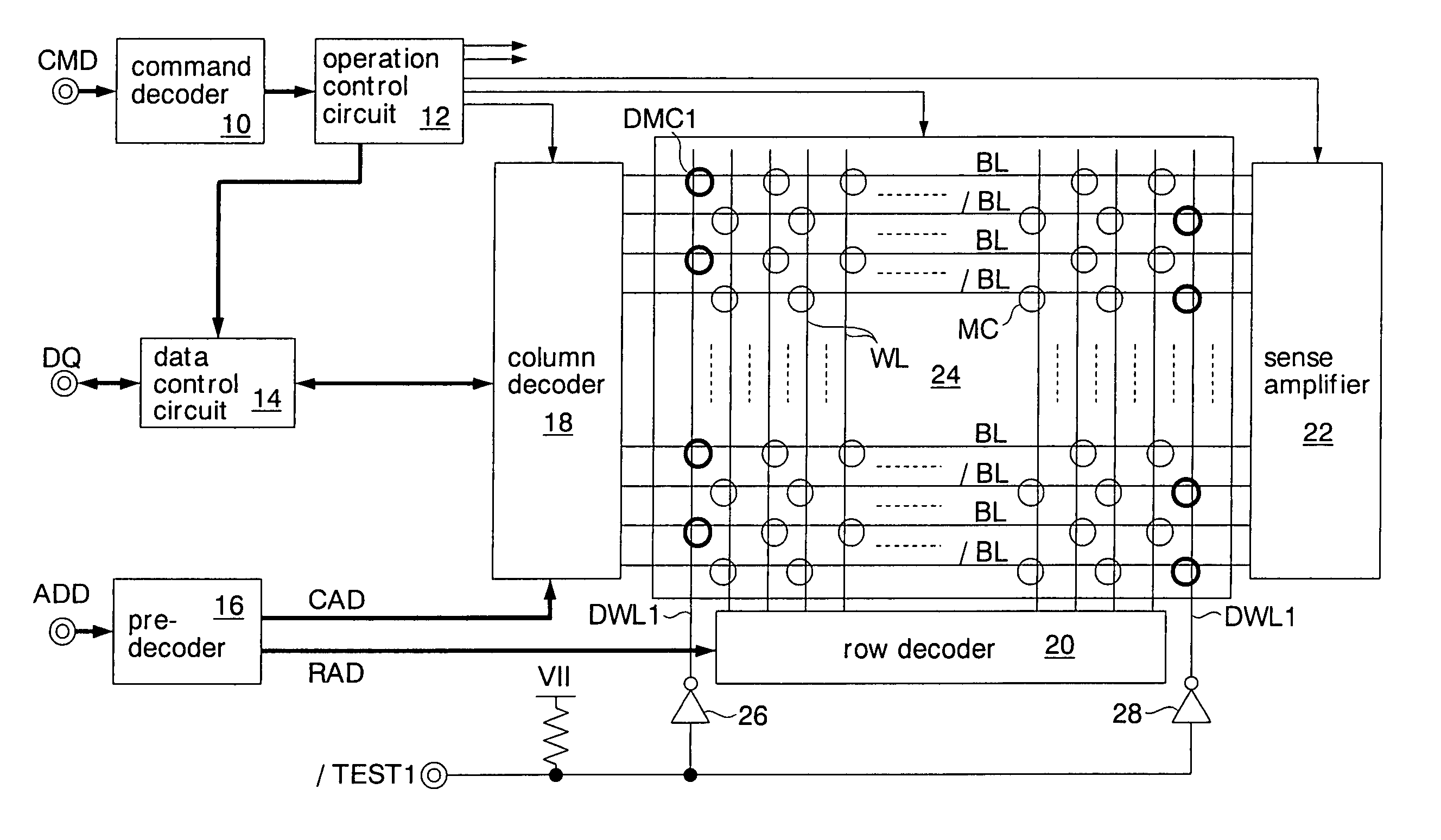
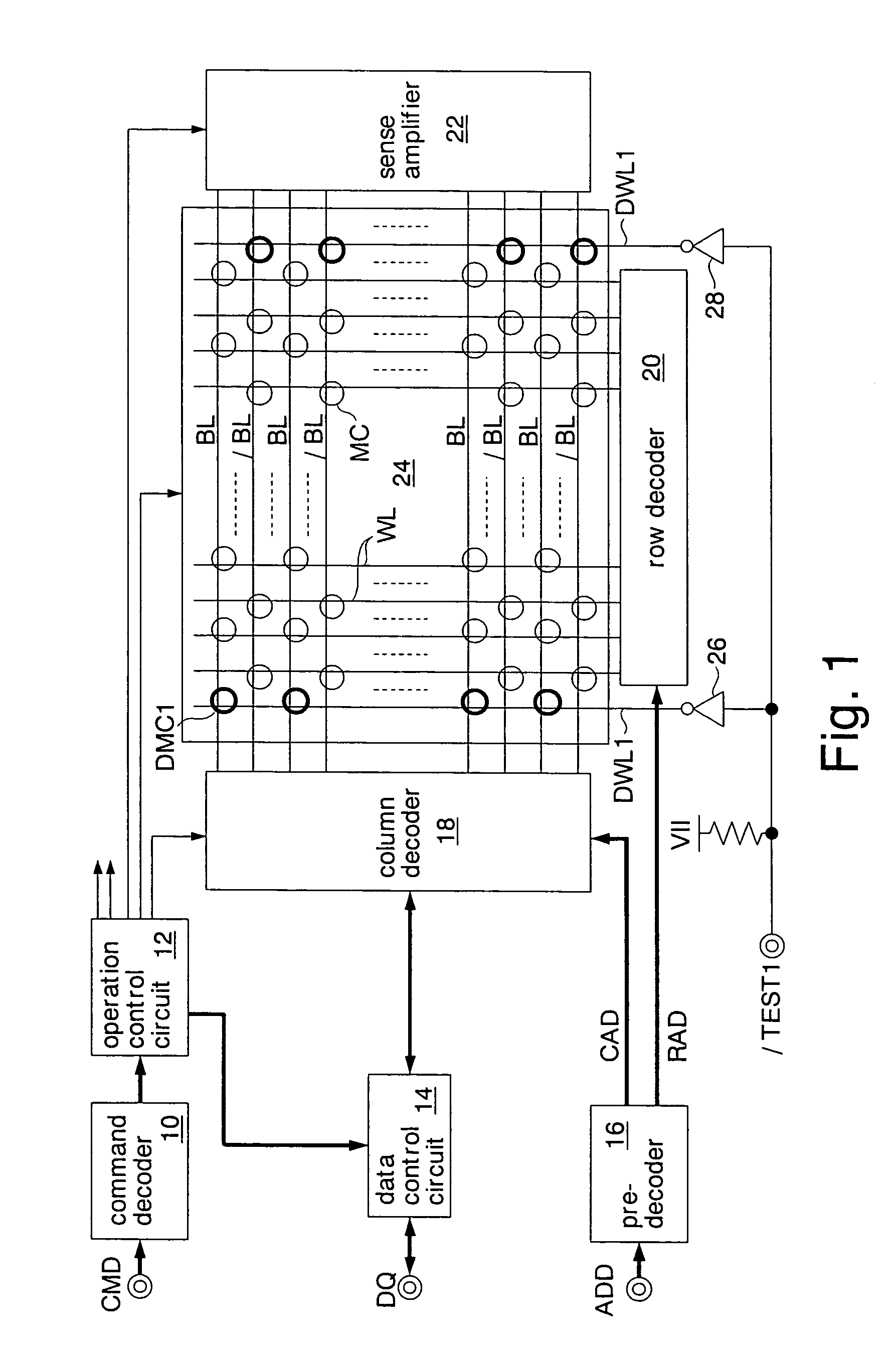
[0032]FIG. 1 shows a semiconductor memory according to the present invention. This semiconductor memory is formed as a DRAM on a silicon substrate by using a CMOS process. The DRAM includes a command decoder 10, an operation control circuit 12, a data control circuit 14, a pre-decoder 16, a column decoder 18, a row decoder 20, a sense amplifier 22, and a memory cell array 24.

[0033]The command decoder 10 receives a command signal CMD (e.g., a row address strobe signal / RAS, a column address strobe signal / CAS, and a chip select signal / CS) supplied via a command terminal, decodes a command (e.g., an access command (a read command and a write command) and a refresh command) indicated by the received command signal CMD, and outputs an internal command signal corresponding to the decoding result to the operation control circuit 12.

[0034]The operation control circuit 12 generates a plurality of operation control signals for operating the memory cell array 24 in accordance with the intern...

third embodiment

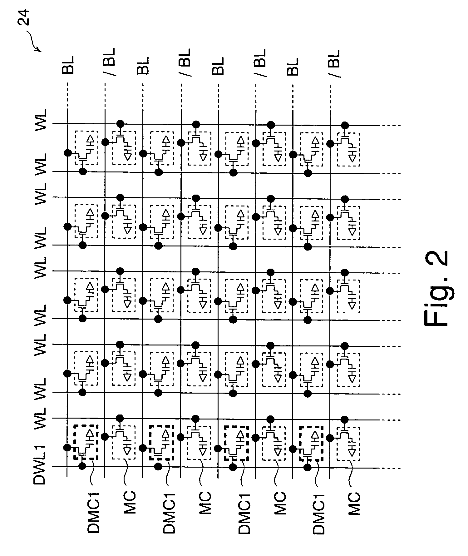
[0074]The memory cell array 24C further includes a dummy bit line DBL2 (the second dummy signal line) on the outside of each dummy bit line DBL1 (the first dummy signal line) of the The outer dummy bit line DBL2 is connected to the precharge voltage line VPR. To the dummy bit line DBL2, dummy memory cells DMC2 (the second dummy memory cells) are connected. The dummy memory cells DMC1 and DMC2 have the same shape (layout) and electric characteristics as those of the real memory cell MC.

second embodiment

[0075]In this embodiment, as in the second embodiment, in order to write data of level H onto the dummy memory cell DMC1 that is required for applying stress to a real memory cell MC, the internal supply voltage VII (level H) is supplied to the dummy bit line DBL1. On the other hand, the dummy bit line DBL2, that is connected to the dummy memory cells DMC2 onto which data of level H is not to be written, is connected to the precharge voltage line VPR. Since the dummy bit line DBL2 is not driven, the drivability of the inverters 30 and 32 can be made small, thus reducing the chip size of the DRAM.

[0076]In this embodiment, the same effects as those described in the first, second, and third embodiments can be also achieved.

[0077]In the aforementioned embodiments, an example has been described in which the present invention is applied to a DRAM. However, the present invention is not limited thereto. For example, the present invention may be applied to other semiconductor memories, such ...


PUM


Abstract

First dummy memory cells connected to a first dummy signal line have the same shape and characteristics as those of a real memory cell. The first dummy memory cells are arranged to be adjacent to outermost real memory cells. A voltage setting circuit changes the voltage of the first dummy signal line from a first voltage to a second voltage in order to write test data onto the first dummy memory cell during a test mode. By writing data of a logic opposite to that of the test data onto the real memory cell adjacent to the first dummy memory cell by means of an operation control circuit, a leak failure that may occur between the first dummy memory cell and the real memory cell adjacent thereto can be checked.

Description

CROSS REFERENCE TO RELATED APPLICATION[0001]This application is based upon and claims the benefit of priority from Japanese Patent Application No. 2004-148000, filed on May 18, 2004, the entire contents of which are incorporated herein by reference.BACKGROUND OF THE INVENTION[0002]1. Field of the Invention[0003]The present invention relates to a technique for surely detecting a failure of a memory cell of a semiconductor memory.[0004]2. Description of the Related Art[0005]A memory cell array of a semiconductor memory includes a plurality of memory cells arranged in a matrix and wirings (word lines and bit lines) for connecting those memory cells to a word decoder, a sense amplifier, and the like. In the memory cell array, elements and wirings are arranged with higher density, as compared with those in circuits near the memory cell array. In other words, the layout density of the elements and wirings on the inside of the memory cell array is different from that on the outside thereof...

Claims


Application Information

Patent Timeline
Patent Type & Authority Patents(United States)
IPC IPC(8): G11C7/00G01R31/28G11C5/00G11C7/02G11C7/14G11C11/401G11C11/4099G11C29/00G11C29/06G11C29/24
CPCG11C7/14G11C29/24G11C29/50G11C11/4099G11C11/401G11C2029/5006
Inventor YAMADA, SHINICHIFUJIEDA, WAICHIROIKEMASU, SHINICHIROH
Owner SOCIONEXT INC
Why Eureka
Try Eureka