
System and method for charge-balanced, continuous-write mask and wafer process for improved colinearity
a write mask and continuous write technology, applied in the manufacture of flux-sensitive heads, magnetic recording, thin film heads, etc., can solve the problems of increasing colinearity errors, image placement errors, and insignificant contributors to the overall control of stripe height, so as to minimize write time, minimize write time, and maximize resolution and image edge fidelity
- Summary
- Abstract
- Description
- Claims
- Application Information
AI Technical Summary
Benefits of technology
Problems solved by technology
Method used
Image

Examples
Embodiment Construction
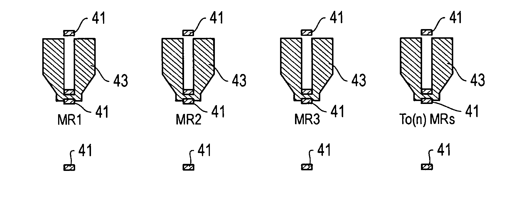
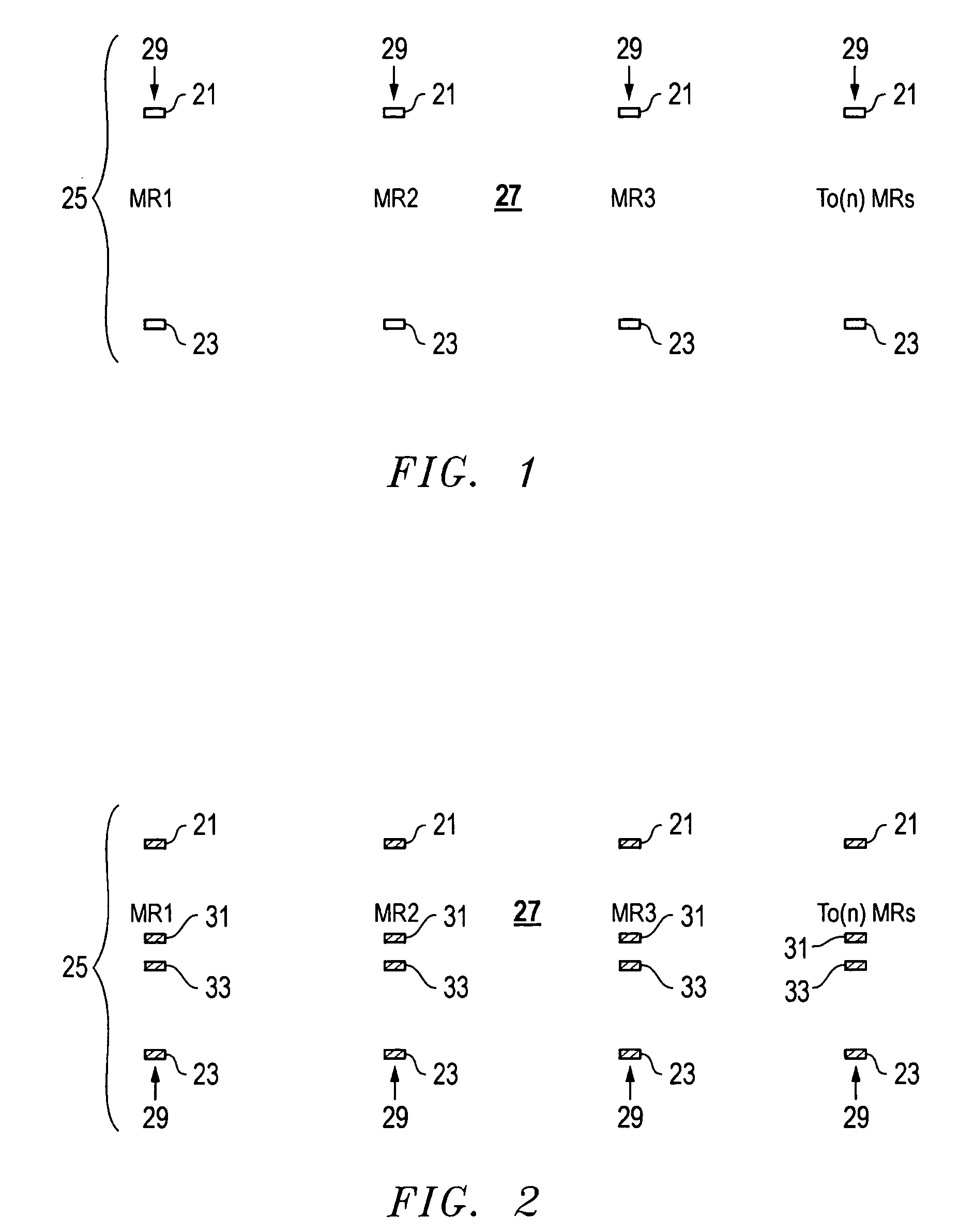
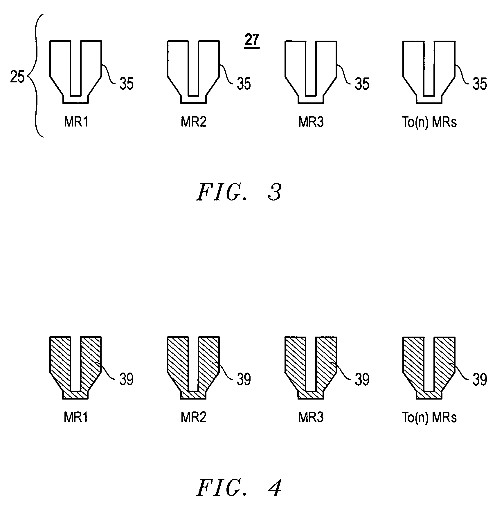
[0032]Referring to FIGS. 1–10, one embodiment of a system and method for a charge-balanced, continuous write mask and wafer process is shown. The first step is to write “charge-balancing” features 21, 23 in order to build a critical negative image magneto resistive (MR) stripe defining field. In this disclosure, although a single mask background and foreground is preferred, a double mask may be used. The system of the present invention has several fields, including foreground in one, test sites in continuous write mode in another, background non-critical targets in another, critical targets in another, etc.
[0033]In the prior art, design systems required designers to design in correct positive, correct negative, reverse positive, reverse negative format considering the use of negative or positive photo-resist. Thereafter the post-processing programs are given instructions to write as correct positive, correct negative, reverse positive, and reverse negative depending on what is wante...
PUM
| Property | Measurement | Unit |
|---|---|---|
| charge- | aaaaa | aaaaa |
| charge-balancing | aaaaa | aaaaa |
| size | aaaaa | aaaaa |
Abstract
Description
Claims
Application Information