Integrated library core for embedded passive components and method for forming electronic device thereon

Inactive Publication Date: 2007-03-13
PHOENIX PRECISION TECH CORP
View PDF14 Cites 19 Cited by
  • Summary
  • Abstract
  • Description
  • Claims
  • Application Information

AI Technical Summary

Benefits of technology

[0017]Therefore, the library core for embedded passive components according to the invention can be used to provide desirable electrical functions for an electronic device such as semiconductor packaging substrate or printed circuit board. The electrically conductive layers on the core layer are patterned to form predetermined conductive traces prior to applying the library core to the semiconductor packaging substrate or printed circuit board; this can prevent the use of complex fabrication processes for mounting or embedding passive components in a conventional multi-layer circuit board, and reduce fabrication costs significantly for the multi-layer circuit board as not having to design or laminate the multi-layer circuit board again, in response to different requirements for electrical characteristics such as resistance and capacitance. Moreover, the library core for embe

Problems solved by technology

In accordance with high integration of the semiconductor device, more leads and circuits are required, which may increase the occurrence of noise.
This thereby requires a relatively large substrate and undesirably enlarges overall dimensions of the semiconductor device; moreover, mounting the passive components respectively on the substrate also increases complexity of circuit arrangement and fabrication for the semiconductor device.
Therefore, if the above conventional arrangements were employed to incorporate more semiconductor chips 11 and passive components 12 on the substrate 1 necessarily to achieve enhanced performances of the semiconductor device, it would not only increase fabrication complexity but also significantly enlarge the dimensions of the semiconductor device, thereby not facilitating dimensions miniaturization of semiconductor packages.
However, due to surface roughness of the organic insulating layer beneath the passive components, it would be hard to achieve desirab

Method used


Image

  • Integrated library core for embedded passive components and method for forming electronic device thereon
  • Integrated library core for embedded passive components and method for forming electronic device thereon
  • Integrated library core for embedded passive components and method for forming electronic device thereon

Examples


Embodiment Construction

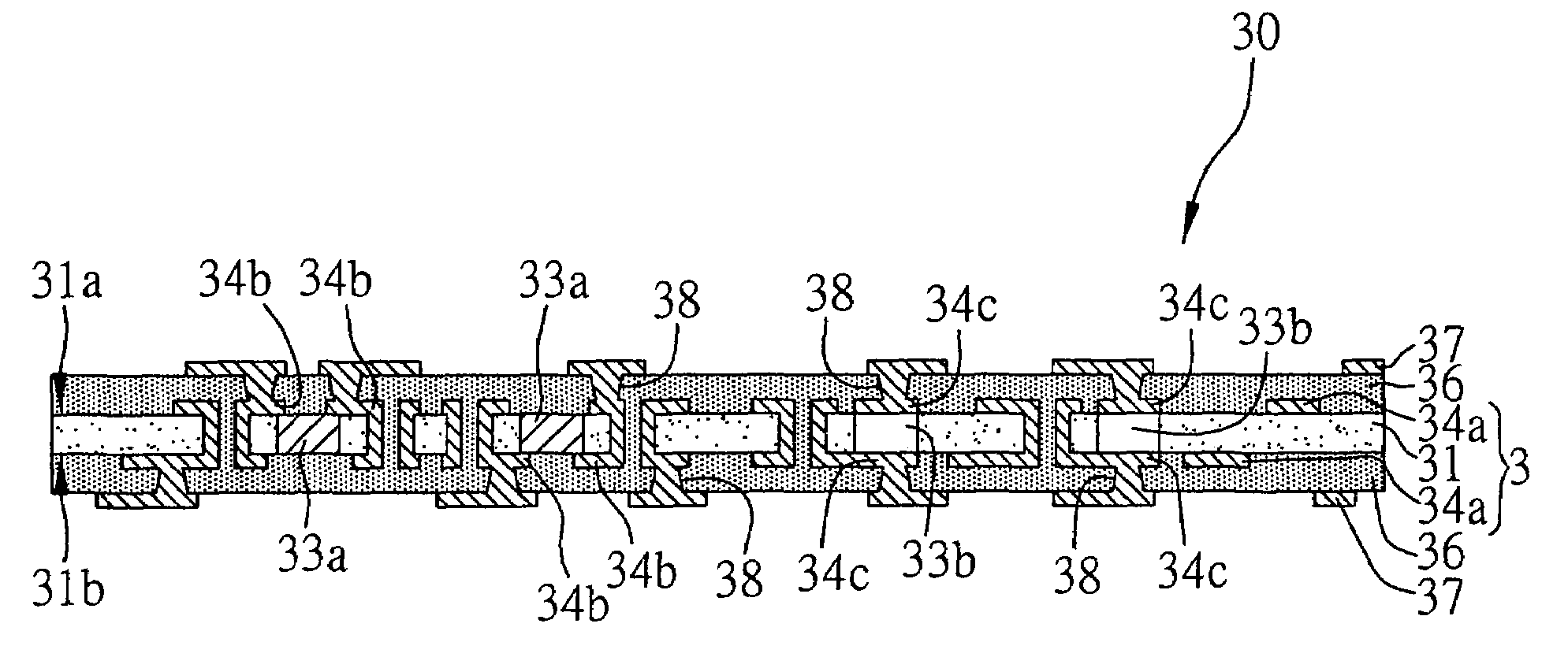
[0029]FIGS. 3A and 3B illustrate an integrated library core for embedded passive components proposed in the present invention.

[0030]As shown in the drawings, this library core 3 primarily includes: an insulating core layer 31 having an upper surface 31a and a lower surface 31b opposed to the upper surface 31a, and formed with a plurality of openings 32 penetrating through the core layer 31; a plurality of areas 33 provided for embedded passive components and defined by the openings 32 of the insulating core layer 31 filled with passive component materials therein; and electrically conductive layers 34 formed over the upper and lower surfaces 31a, 31b of the core layer 31 respectively, wherein the electrically conductive layers 34 cover the areas 33 for forming the passive components contained within the openings 32 of the core layer 31. The library core 3 is further formed with a plurality of conductive vias 35 for electrically interconnecting the electrically conductive layers 34 r...


PUM

PropertyMeasurementUnit
Electrical conductivityaaaaaaaaaa
Electrical conductoraaaaaaaaaa

Abstract

An integrated library core for embedded passive components and a method for forming an electronic device on the library core are provided. An insulating core layer is formed with a plurality of openings penetrating therethrough and with electrically conductive layers on upper and lower surfaces thereof. The openings of the core layer are filled with materials for forming passive components such as resistors and capacitors. This thereby provides an integrated library core on which the electrically conductive layers of the core layer can be desirably patterned to electrically interconnect the passive components, and this library core can be electrically connected to an electronic device such as substrate or printed circuit board to enhance performances of electrical characteristics for the electronic device.

Description

FIELD OF THE INVENTION[0001]The present invention relates to an integrated library core for embedded passive components and methods for forming an electronic device on the library core, and more particularly, to a library core having an insulating core layer embedded with a plurality of capacitive and resistive materials, and a fabrication method for connecting the library core for forming an electronic device.BACKGROUND OF THE INVENTION[0002]Owing to the progress of semiconductor packaging technology and improvements in performances of electrical characteristics for semiconductor chips, semiconductor devices are developed to higher integration. In exemplification of a BGA (ball grid array) semiconductor package, a plurality of array-arranged solder balls are mounted on a bottom surface of a substrate and used as input / output (I / O) connections for electrically connecting a semiconductor chip mounted on the substrate to an external device such as printed circuit board (PCB). Compared...

Claims


Application Information

Patent Timeline
IPC IPC(8): H01K1/18H01L23/64H05K1/09H05K1/16H05K3/40H05K3/42H05K3/46
CPCH01L23/5389H01L23/642H01L23/647H05K1/162H05K1/167H01L23/49822H01L2224/16235H01L2224/16H01L2224/48091H01L2224/48227H01L2924/01029H01L2924/01078H01L2924/04941H01L2924/15153H01L2924/1517H01L2924/15311H01L2924/1532H01L2924/19041H05K1/092H05K1/095H05K3/4061H05K3/4069H05K3/426H05K3/4602H05K2201/0187H05K2201/09536H01L23/50H01L24/48H01L2924/00014H01L24/49H01L2224/05599H01L2224/45099H01L2224/49175H01L2224/85399H01L2924/19105
Inventor HU, CHU-CHIN
Owner PHOENIX PRECISION TECH CORP
Why Eureka
Try Eureka