
OLED device using reduced drive voltage

a technology of oled and drive voltage, which is applied in the direction of discharge tube luminescnet screen, other domestic articles, natural mineral layered products, etc., can solve the problems of diffusive metals and luminescence quenching in oleds, and achieve high operational stability, reduce the drive voltage of the oled, and high luminous efficiency

Active Publication Date: 2007-03-20
GLOBAL OLED TECH
View PDF14 Cites 95 Cited by
  • Summary
  • Abstract
  • Description
  • Claims
  • Application Information

AI Technical Summary

Benefits of technology

[0019]It is an advantage of this invention that the drive voltage of the OLED can be reduced, while maintaining the desired color of light emission. It is a further advantage that an OLED device made in accordance with this invention has high luminous efficiency and high operational stability. It is a further advantage that the color of light emission can be tuned to achieve a desired color.

Problems solved by technology

However, Li and other metals are reported as being diffusive in organic layers resulting in luminescence quenching in OLEDs, for example, as reported by Haskal et al. in “Lithium-Aluminum Contacts for Organic Light-Emitting Devices”, Applied Physics Letters, 71, 1151 (1997).

Method used


Image

  • OLED device using reduced drive voltage
  • OLED device using reduced drive voltage
  • OLED device using reduced drive voltage

Examples


example 3 (

Inventive)

[0220]An OLED device was constructed in the manner described in Example 1, Steps 1–5; Steps 6–10 were as follows:[0221]6. A 10 nm layer of tris(8-quinolinolato)aluminum (III) (ALQ) was vacuum-deposited onto the substrate at a coating station that included a heated graphite boat source to form a green light-emitting layer;[0222]7. A 10 nm metal-doped organic layer of tris(8-quinolinolato)-aluminum (III) (ALQ) with 1.5% Li was vacuum-deposited onto the substrate at a coating station that included a heated graphite boat source;[0223]8. A 15 nm electron-transporting layer (ETL) of tris(8-quinolinolato)-aluminum (III) (ALQ) was vacuum-deposited onto the substrate at a coating station that included a heated graphite boat source;[0224]9. A 0.5 nm layer of lithium fluoride was evaporatively deposited onto the substrate, followed by a 100 nm layer of aluminum, to form a cathode layer; and[0225]10. The device was then transferred to a dry box for encapsulation.

example 4 (

Inventive)

[0226]An OLED device was constructed in the manner described in Example 1, Steps 1–5; Steps 6–10 were as follows:[0227]6. A 20 nm layer of tris(8-quinolinolato)aluminum (III) (ALQ) was vacuum-deposited onto the substrate at a coating station that included a heated graphite boat source to form a green light-emitting layer;[0228]7. A 10 nm metal-doped organic layer of tris(8-quinolinolato)-aluminum (III) (ALQ) with 1.5% Li was vacuum-deposited onto the substrate at a coating station that included a heated graphite boat source;[0229]8. A 5 nm electron-transporting layer (ETL) of tris(8-quinolinolato)-aluminum (III) (ALQ) was vacuum-deposited onto the substrate at a coating station that included a heated graphite boat source;[0230]9. A 0.5 nm layer of lithium fluoride was evaporatively deposited onto the substrate, followed by a 100 nm layer of aluminum, to form a cathode layer; and[0231]10. The device was then transferred to a dry box for encapsulation.

example 6 (

Inventive)

[0236]An OLED device was constructed in the manner described in Example 1, Steps 1–5; Steps 6–9 were as follows:[0237]6. A 10 nm layer of tris(8-quinolinolato)aluminum (III) (ALQ) was vacuum-deposited onto the substrate at a coating station that included a heated graphite boat source to form a green light-emitting layer;[0238]7. A 25 nm metal-doped organic layer of tris(8-quinolinolato)-aluminum (III) (ALQ) with 1.5% Li was vacuum-deposited onto the substrate at a coating station that included a heated graphite boat source;[0239]8. A 100 nm layer of aluminum was evaporatively deposited onto the substrate to form a cathode layer; and[0240]9. The device was then transferred to a dry box for encapsulation.

Results (Examples 1–6)

[0241]The devices were tested by applying a current across the electrodes of 20 mA / cm2 and measuring the spectrum. The relative luminous efficiency is defined as the luminous efficiency of the example device, in cd / A, divided by the luminous efficiency ...


PUM

PropertyMeasurementUnit
thicknessaaaaaaaaaa
work functionaaaaaaaaaa

Abstract

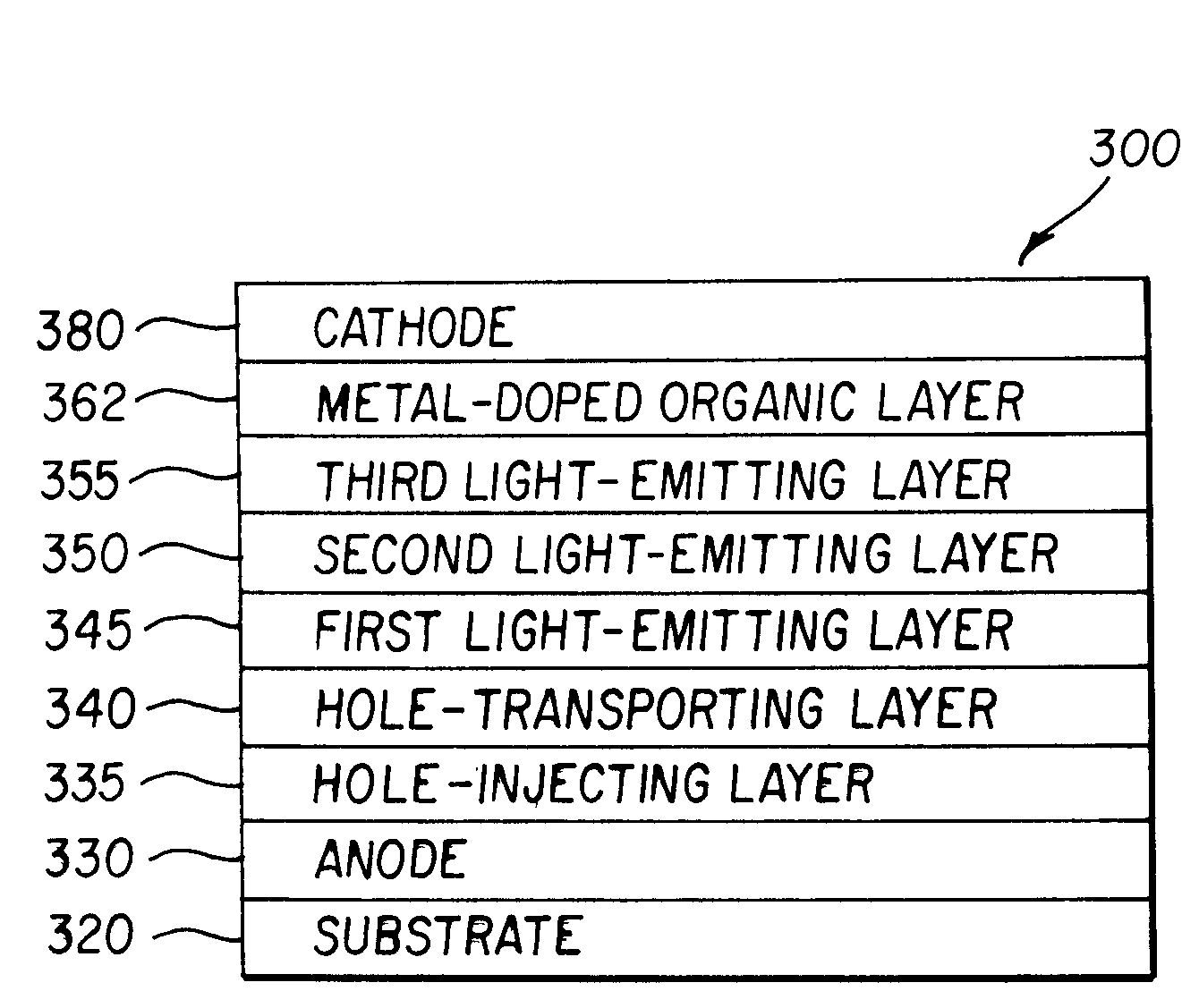
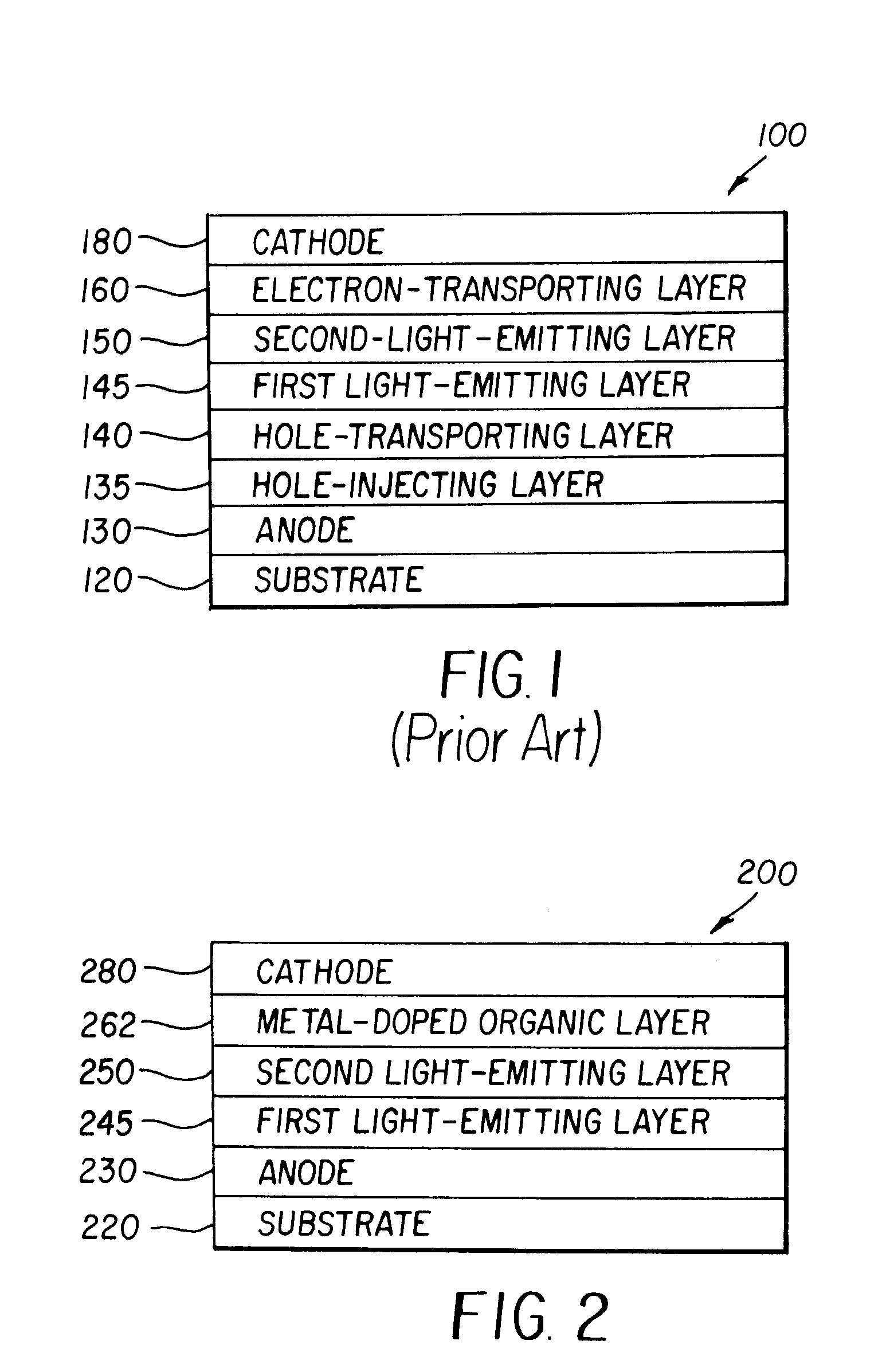
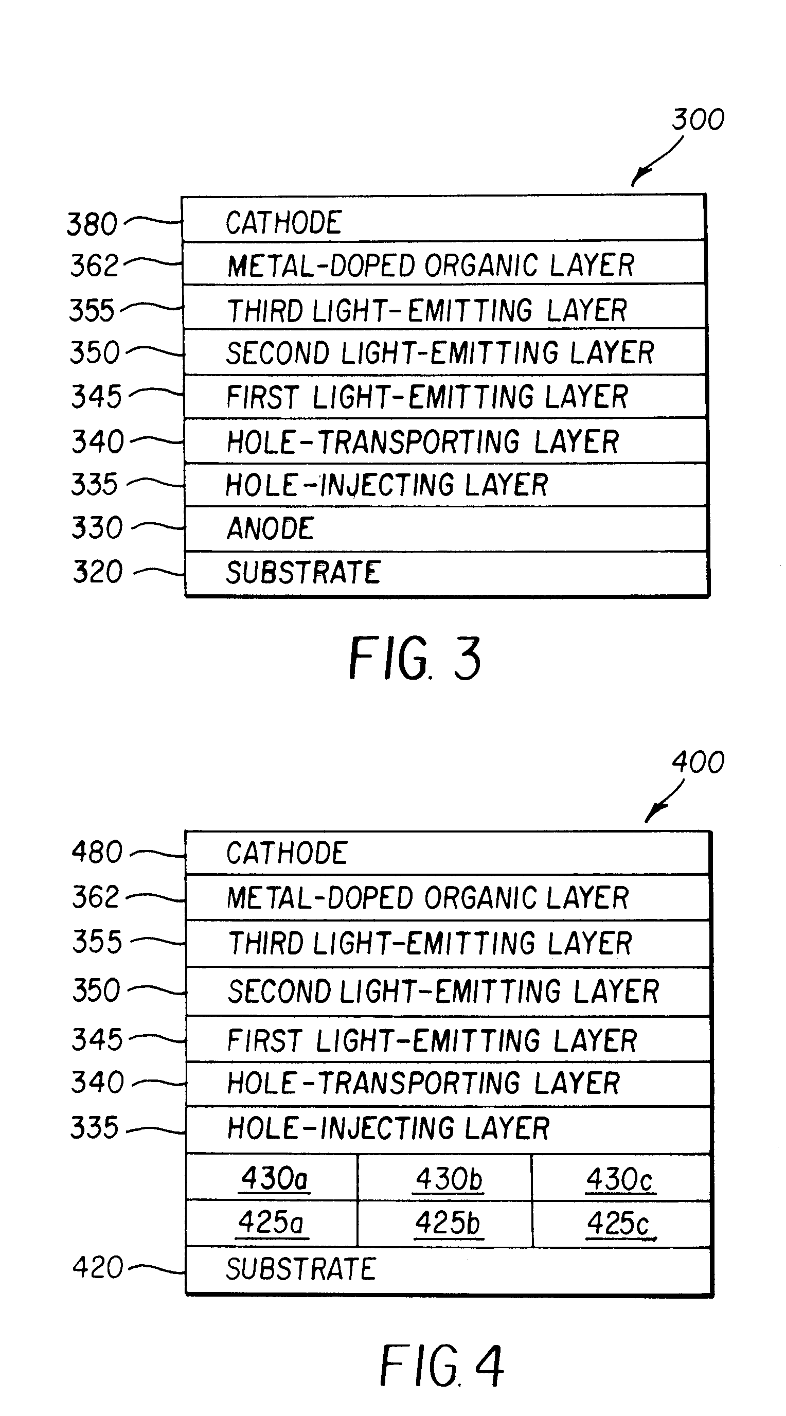
An OLED device includes an anode, a first light-emitting layer disposed over the anode, and a second light-emitting layer disposed over the first light-emitting layer. The device also includes a metal-doped organic layer containing an organic electron-transporting material and a low work function metal disposed over the second light-emitting layer, and a cathode disposed over the metal-doped organic layer.

Description

CROSS REFERENCE TO RELATED APPLICATIONS[0001]Reference is made to commonly assigned U.S. patent application Ser. No. 10 / 713,523 filed Nov. 14, 2003 by Liang-Sheng Liao et al., entitled “Organic Electroluminescent Devices Having a Stability-Enhancing Layer”, the disclosure of which is herein incorporated by reference.FIELD OF THE INVENTION[0002]The present invention relates to reducing drive voltages for organic electroluminescent (EL) devices, also known as organic light-emitting diodes (OLED) that emit color light.BACKGROUND OF THE INVENTION[0003]An organic light-emitting diode device, also called an OLED device, commonly includes a substrate, an anode, a hole-transporting layer made of an organic compound, an organic luminescent layer with suitable dopants, an organic electron-transporting layer, and a cathode. OLED devices are attractive because of their low driving voltage, high luminance, wide-angle viewing and capability for full-color flat emission displays. Tang et al. descr...

Claims


Application Information

Patent Timeline
Patent Type & Authority Patents(United States)
IPC IPC(8): H01L51/50H05B33/14H05B33/12
CPCH01L51/5036H01L51/5052Y10S428/917H01L51/5092H10K50/125H10K50/165H10K50/171
Inventor RICKS, MICHELE L.HATWAR, TUKARAM K.SPINDLER, JEFFREY P.BOROSON, MICHAEL L.
Owner GLOBAL OLED TECH
Learn More