Distributed link module architecture

Inactive Publication Date: 2007-03-20
HEWLETT PACKARD DEV CO LP
View PDF4 Cites 7 Cited by
  • Summary
  • Abstract
  • Description
  • Claims
  • Application Information

AI Technical Summary

Problems solved by technology

These links typically have high frequency (2 GHz plus) signaling that, due to losses in the transmission media (printed circuit board and connectors), results in small signals being received at the input of the destination chip.
The placement and grouping of these analog blocks are constrained by several issues, wherein the issues include:common analog power supplies;common external reference components;C4 bump density, package routing density, and pin density issues;clock and data skew;placement of the link receiver and transmitters relative to other on-chip input output modules like, for example, the cross bar switch;

Method used


Image

  • Distributed link module architecture
  • Distributed link module architecture
  • Distributed link module architecture

Examples


Embodiment Construction

[0030]The following description of the preferred embodiment(s) is merely exemplary in nature and is in no way intended to limit the invention, its application, or uses.

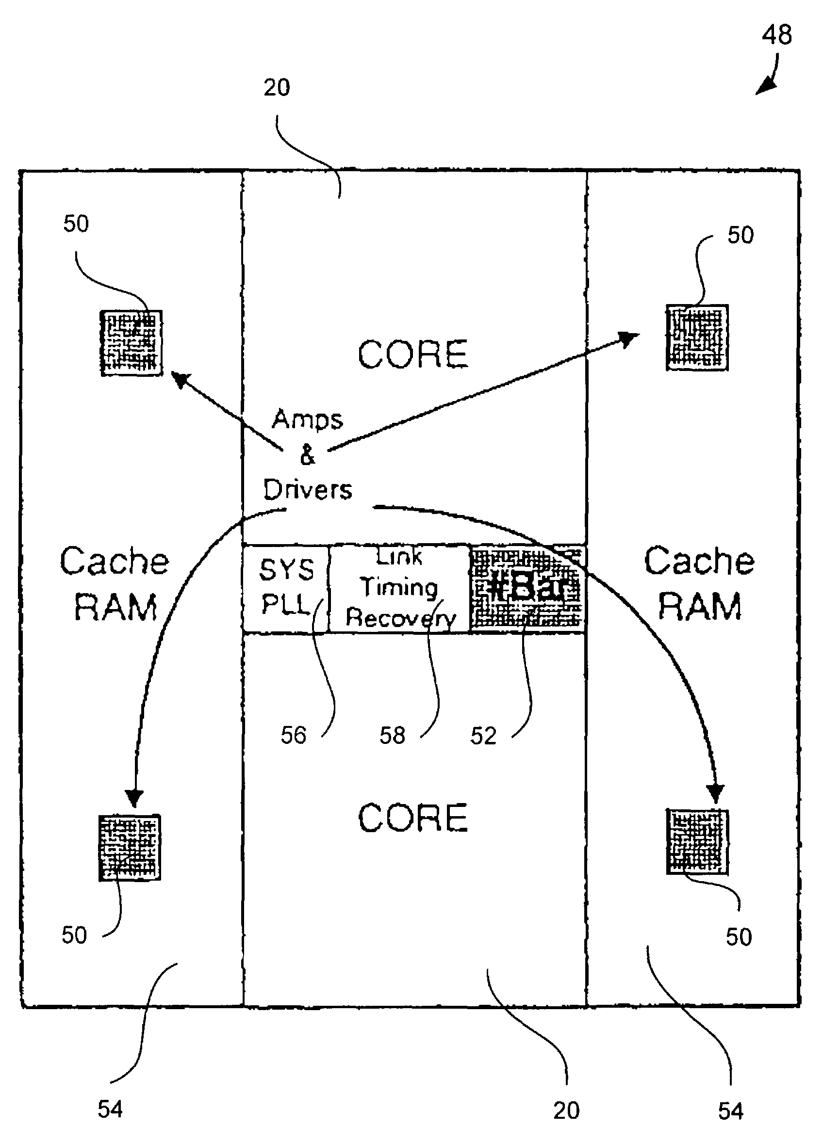
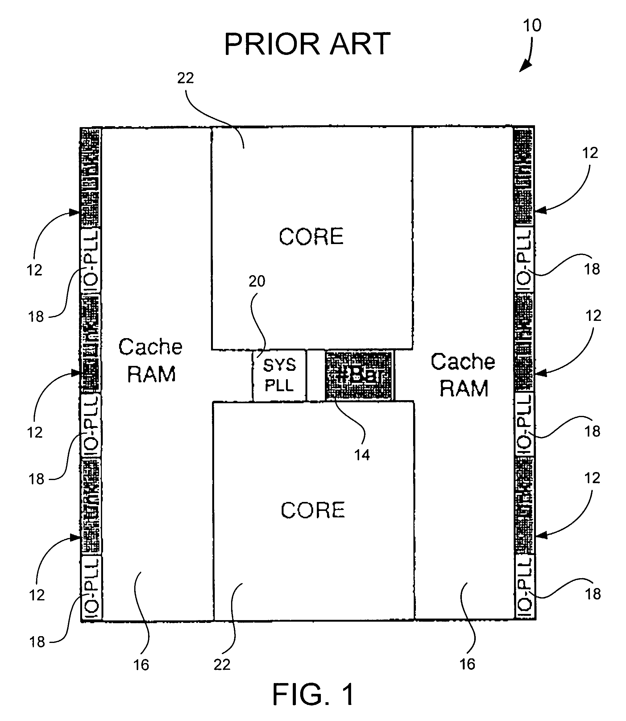
[0031]Referring to FIG. 3, a link layout architecture 48 according to the present invention is shown. In this scheme, only the bit receivers and bit output drivers 50 (with their pre-emphasis circuitry) are placed at a distance from the cross bar switch 52. The remaining link module circuitry for all the links is placed near to the cross bar switch 52. The remote link circuitry is much smaller than the existing methodology, which allows this circuitry to be more easily integrated into the sea of cache random access memory 54. As shown in FIG. 3, the bit receivers and bit output drivers 50 are grouped into 4 regions. There could, however, be more regions since there are no major constraints as to where these remote analog regions could be placed other than the C4 and package constraints. Therefore, these remote analog ...


PUM


Abstract

A link module architecture is disclosed for use with a multi-core central processing unit having a cross bar switch. The link module comprises timing recovery circuitry operably coupled to the central processing unit, wherein the timing recovery circuitry is positioned proximate to the cross bar switch. The link module further comprises a bit receiver operably coupled to the central processing unit, and a bit output driver operably coupled to the central processing unit. The bit receiver, preferably comprising a wide bandwidth amplifier, and the bit driver are preferably integrated with a sea of on-chip RAM.

Description

FIELD OF THE INVENTION[0001]The present invention generally relates to multi-core central processing units and particularly relates to the link layout architecture for a central processing unit.BACKGROUND OF THE INVENTION[0002]New computer architectures, especially those utilizing multiprocessor technologies, use high-speed serial point-to-point link interconnect strategies. These links typically have high frequency (2 GHz plus) signaling that, due to losses in the transmission media (printed circuit board and connectors), results in small signals being received at the input of the destination chip. These small amplitude signals are normally sent differentially to increase the link reliability and reduce the link's sensitivity to common-mode noise. A link module typically consists of one to twenty bits of data operating in bidirectional mode. A link module also typically includes timing recovery circuitry (multi-phase lock loop) and voltage restore circuitry (integrating receivers)....

Claims


Application Information

Patent Timeline
IPC IPC(8): G06F1/00G06F17/50G06F15/16G06F13/36G06F13/42G06F15/78H03L7/06H04J3/06
CPCG06F15/7832H03L7/06H04J3/0685
Inventor KNEE, DEREK L.INDERMAUR, THOMAS N.
Owner HEWLETT PACKARD DEV CO LP
Why Eureka
Try Eureka