
Method of manufacturing a low temperature polysilicon film

a technology of polysilicon and low temperature, applied in the direction of nuclear engineering, transportation and packaging, railway signalling, etc., can solve the problems of reducing the electric property and stability of tft, the nucleation position of the crystallization process is not under control, and the cost of the novel tft technology is much lower than that of the conventional amorphous silicon

Active Publication Date: 2007-03-27
AU OPTRONICS CORP
View PDF3 Cites 10 Cited by
  • Summary
  • Abstract
  • Description
  • Claims
  • Application Information

AI Technical Summary

Benefits of technology

[0007]Accordingly, one object of the present invention is to provide a manufacturing process of low temperature polysilicon TFT in which the position of the crystal grain is controlled by controlling the position of the crystal seed during the nucleation process of the amorphous silicon film.
[0008]It is another object of the present invention to provide a manufacturing process of low temperature polysilicon TFT in which the uniformity of the grain size and the grain distribution in the conventional manufacturing process can be resolved.
[0009]It is another object of the present invention to provide a manufacturing process of low temperature polysilicon TFT in which the number of grain interfaces in the channel of the TFT can be reduced and the number of grain interfaces in the channel of the TFT can be controlled in a predetermined range of all of the TFTs.
[0013]Furthermore, because the grain size and the grain distribution can be controlled, the number of grain interfaces in the channel of the TFT can be reduced, and the electric property and the stability of the TFT will be enhanced.

Problems solved by technology

Thus the cost of the novel TFT technology is much lower than that of the conventional amorphous silicon TFT.
However, the nucleation position of the crystallization process is not under control in the conventional laser crystallization process of transforming the amorphous polysilicon film to the polysilicon film.
In addition, the grain sizes of the crystal are not uniform after the laser crystallization process, thus the number of grain interfaces in the channel of each TFT will be different, and if the number of grain interfaces in the channel is too large, the electric property and the stability of the TFT will be reduced.

Method used


Image

  • Method of manufacturing a low temperature polysilicon film
  • Method of manufacturing a low temperature polysilicon film
  • Method of manufacturing a low temperature polysilicon film

Examples


Embodiment Construction

[0018]The present invention now will be described more fully hereinafter with reference to the accompanying drawings in which preferred embodiments of the invention are shown. The present invention may, however, be embodied in many different forms and should not be construed as limited to the embodiments set forth herein. Rather, these embodiments are provided so that this disclosure will be thorough and complete, and will fully convey the scope of the invention to those skilled in the art. Like numbers refer to like elements throughout. Moreover, each embodiment described and illustrated herein includes its complementary conductivity type embodiment as well.

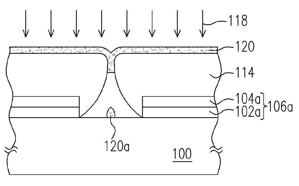
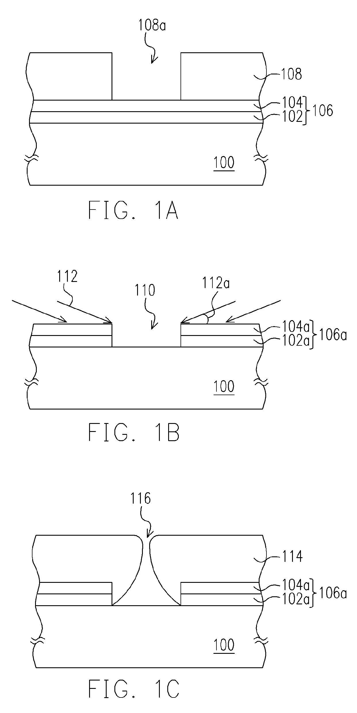
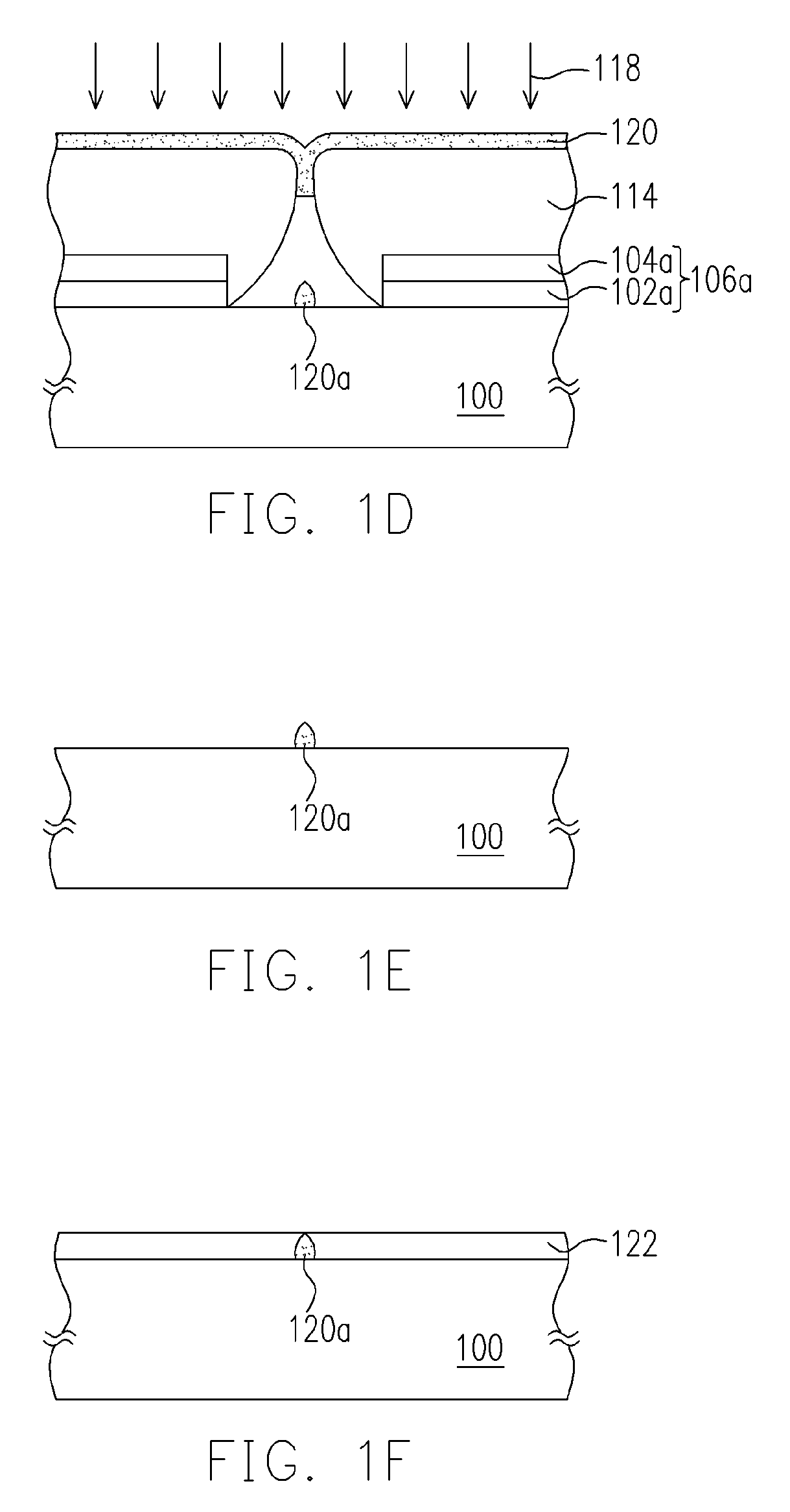
[0019]The present invention provides a manufacturing method of low temperature polysilicon film. FIG. 1A to FIG. 1G schematically illustrate the cross-sectional diagrams of a manufacturing process flow of low temperature polysilicon film of a preferred embodiment of the present invention. Referring to FIG. 1A, there is provided ...


PUM

PropertyMeasurementUnit
Angleaaaaaaaaaa
Angleaaaaaaaaaa
Temperatureaaaaaaaaaa

Abstract

A method of manufacturing a low temperature polysilicon film is provided. A first metal layer is formed on a substrate; and openings have been formed in the first metal layer. A second metal layer is formed on the first metal layer: and a hole corresponding to each of the openings is formed in the second metal layer. A silicon layer is formed on the second metal layer; a silicon seed is formed on the substrate inside each of the holes. After removing the first and the second metal layers, an amorphous silicon layer is formed on the substrate by using the silicon seed. Then a laser crystallization step is performed to form a polysilicon layer from the amorphous layer. Since the position of the silicon seed can be controlled, the size and distribution of the silicon grain and the number of the silicon crystal interface can also be controlled.

Description

CROSS REFERENCE TO RELATED APPLICATIONS[0001]This application claims the priority benefit of Taiwan application serial no. 92107061, filed Mar. 28, 2003.BACKGROUND OF INVENTION[0002]1. Field of the Invention[0003]The present invention relates to a low temperature polysilicon film. More particularly, the present invention relates to a method for controlling the nucleation position of the crystallization of the low temperature polysilicon film.[0004]2. Description of the Related Art[0005]In the development of the process of the thin film transistor (TFT) liquid crystal display (LCD), a technology of low temperature polysilicon TFT has become a trend in recent years. The technology of low temperature polysilicon TFT is a novel TFT technology compared with conventional amorphous silicon TFT. The electronic mobility of the novel TFT technology has been at least up to 200 cm2 / V-sec, and therefore the size of the chip area is reduced and the aperture ratio is increased. Moreover, because o...

Claims


Application Information

Patent Timeline
IPC IPC(8): B05D5/00B05D3/00C23C16/00C23C16/02C23C16/24
CPCC23C16/24C23C16/02
Inventor WUNG, CHIEN-SHENCHANG, MAO-YICHANG, CHIH-CHIN
Owner AU OPTRONICS CORP
Learn More