Method for setting design margin for LSI

a design margin and design technology, applied in the field of setting design margins, can solve the problems of difficult to set an appropriate design margin against the fabrication variation, difficult to efficiently develop an optimum lsi, waste of circuit design on the contrary, etc., and achieve the effect of suppressing the setting of excessive or insufficient design margins and more realistic and accura

Active Publication Date: 2007-03-27
PANNOVA SEMIC
View PDF4 Cites 17 Cited by
  • Summary
  • Abstract
  • Description
  • Claims
  • Application Information

AI Technical Summary

Benefits of technology

[0056]Thus, the difference between the actual delay yield of the LSI actually fabricated on the basis of the specific design margin set in the aforementioned manner and the delay yield predicted before the fabrication can be made to influence the design margin against the fabrication variation and the delay yield of LSIs to be fabricated thereafter. Accordingly, the design margin to be set for the LSIs to be developed thereafter can be more realistic and accurate. As a result, setting of an excessive or insufficient design margin can be suppressed.

Problems solved by technology

The quality of an LSI can be safely secured by excessively setting a design margin for the LSI, but although it is thus safely secured, the circuit design may become wasteful on the contrary.
Accordingly, without a technique to evaluate not excessive but appropriate design margin and to design an LSI on the basis of the evaluated design margin, it is difficult to efficiently develop an optimum LSI, such as a recent digital signal processor, satisfactory in both the performance and the quality.
However, it is not easy to set an appropriate design margin against the fabrication variation because the occurrence mechanism of the fabrication variation is complicated.
Specifically, the variation derived from the voltage or the temperature can be set on the basis of response of a circuit to one variable while there are a large number of variables (process variables) for determining the fabrication variation, and therefore, it is difficult to set a design margin against the fabrication variation.
However, in the conventional method for setting a design margin for an LSI, since the corner condition (the upper and lower limits) of the SPICE parameter to be used in the SPICE simulation is determined on the basis of the variation specifications 20 of the process variables shown in FIG. 22, a combination of specification values actually minimally possible is used.
However, there is very small probability that these process variations are simultaneously the maximum, and hence, such a combination is actually minimally possible.
Therefore, the derating factor calculated on the basis of the delay time calculated through the SPICE simulation tends to have an excessive value.
In other words, in the conventional method, an excessive design margin tends to be set.
Therefore, the design margin set by the conventional method may have an excessive or insufficient value.

Method used


Image

  • Method for setting design margin for LSI
  • Method for setting design margin for LSI
  • Method for setting design margin for LSI

Examples


embodiment 1

[0080]Now, a method for setting a design margin for an LSI according to Embodiment 1 of the invention will be described with reference to the accompanying drawings.

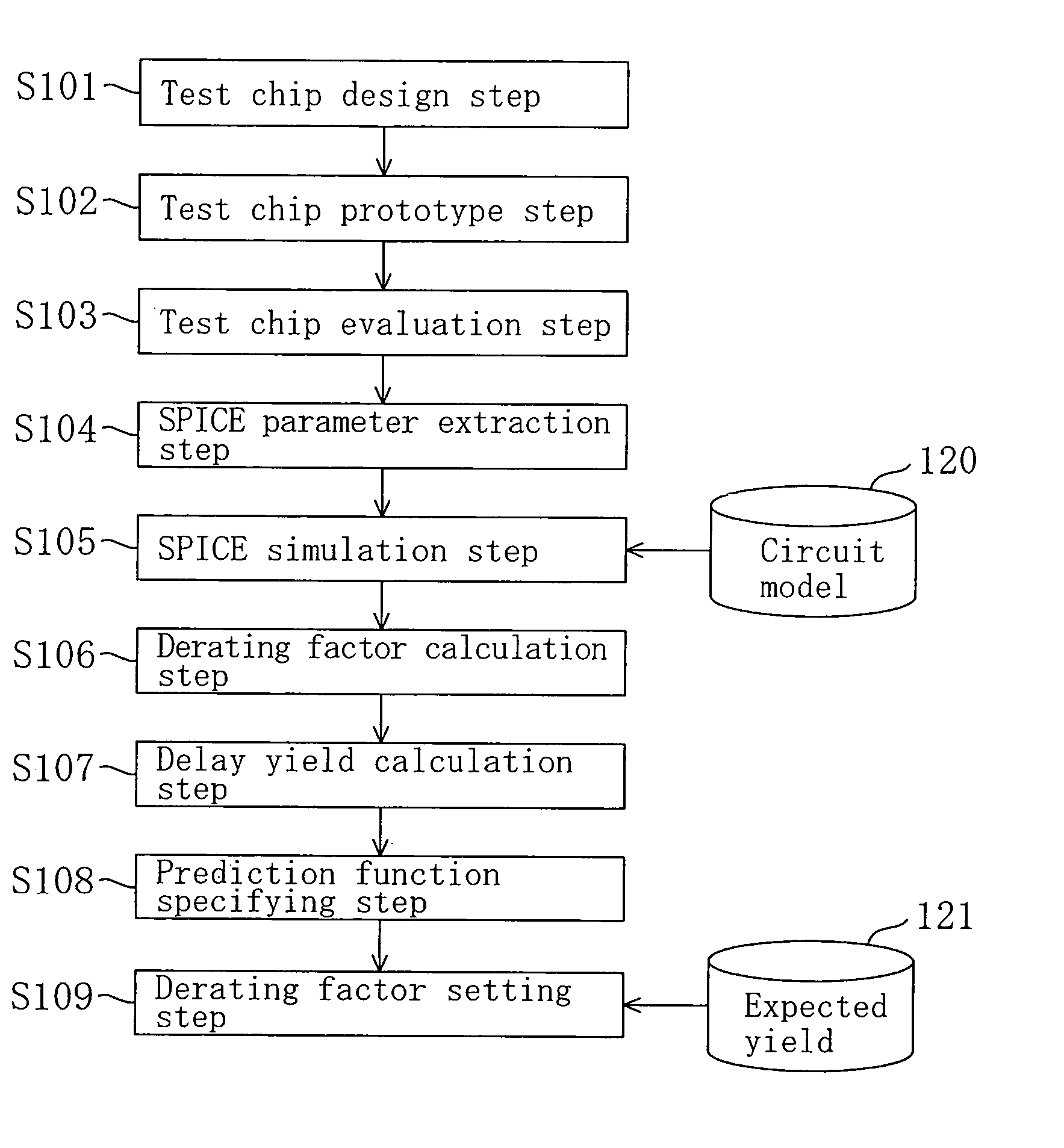
[0081]FIG. 1 is a diagram for showing procedures in the method for setting a design margin for an LSI of Embodiment 1. In the method of this embodiment, a design margin is set against fabrication variation with the fabrication variation of a CMOS transistor, that is, a kind of CMIS transistor, regarded as a delay varying factor.

[0082]As shown in FIG. 1, first in a test chip design step S101, a test chip mounting a variety of transistors to be included in an LSI to be fabricated is designed.

[0083]Next, in a test chip prototype step S102, a plurality of test chips designed in the test chip design step S101 are prototyped.

[0084]Then, in a test chip evaluation step S103, transistor characteristics, that is, for example, at least current-voltage characteristics, of NMOS transistors and PMOS transistors out of the various trans...

embodiment 2

[0119]Now, a method for setting a design margin for an LSI according to Embodiment 2 of the invention will be described with reference to the accompanying drawings.

[0120]As a characteristic of Embodiment 2, a design margin against the fabrication variation is set by taking not only the variation component of the transistor characteristic described in Embodiment 1 but also a variation component of the wiring characteristic of the LSI into consideration as the delay varying factor of the logic circuit included in the LSI.

[0121]Therefore, the characteristic part of this embodiment will be described particularly in detail.

[0122]FIG. 1 is a diagram for showing procedures in the method for setting a design margin for an LSI of Embodiment 2, in particular, in which the design margin against the fabrication variation is set by regarding, as the delay varying factor, the variation component of the characteristic of a CMOS transistor, that is, a kind of CMIS transistor and the variation compo...

embodiment 3

[0144]A method for setting a design margin for an LSI according to Embodiment 3 of the invention will now be described with reference to the accompanying drawings.

[0145]FIG. 13 is a diagram for showing procedures in the method for setting a design margin for an LSI according to Embodiment 3. In Embodiment 3 shown in FIG. 13, the same procedures as those shown in FIG. 1 of the method for setting a design margin for an LSI according to Embodiment 1 are referred to by using the same reference numerals.

[0146]As shown in FIG. 13, as a characteristic of this embodiment, the method of this embodiment includes, in addition to the procedures up to the setting of a design margin described in Embodiment 1, a product development / mass-production step S301 of developing and mass-producing a product on the basis of the set design margin and a delay yield verification step S302 of correcting the design margin on the basis of the LSI actually fabricated as a product.

[0147]Specifically, in the produc...


PUM


Abstract

After predicting a relationship between a design margin set against a fabrication variation in design of an LSI and a yield, a specific design margin for attaining a given yield is calculated based on the predicated relationship. The yield is a delay yield obtained by cumulating a signal propagation delay time thereby achieving a probability that a signal propagated through a logic circuit of the LSI is delayed by a given amount of time, and the design margin is a derating factor indicating a ratio between the signal propagation delay time and a standard value of the signal propagation delay time.

Description

BACKGROUND OF THE INVENTION[0001]The present invention relates to a technique to set a design margin to be employed, in design of an ASIC (Application Specific IC), a system LSI or the like, for taking performance variation derived from variation in the fabrication process into consideration.[0002]Recently, since transistors are rapidly improved in the refinement and the degree of integration in accordance with the development of fabrication technique, a variety of functions can be realized on one chip of a CMIS (Complementary Metal Insulator Semiconductor) integrated circuit (hereinafter referred to as the LSI). In the development of such an LSI, a design margin is generally provided. Factors to be considered in setting the design margin include, as factors that affect the circuit characteristics, not only the voltage and the temperature corresponding to the operation circumstances of the circuit but also variation or fluctuation occurring in the fabrication. Signal propagation del...

Claims


Application Information

Patent Timeline
Patent Type & Authority Patents(United States)
IPC IPC(8): G06F17/50H01L21/82H01L29/00
CPCG06F17/5036G06F30/367
Inventor YONEZAWA, HIROKAZU
Owner PANNOVA SEMIC
Why Eureka
Try Eureka