Systems configured to provide illumination of a specimen during inspection

a technology of specimen illumination and illumination, applied in the field of systems configured to provide specimen illumination during inspection, can solve the problems of increasing the difficulty of achieving both high resolution and a long field, and the need to detect defects of decreasing size, and achieve the effect of large working distan

Active Publication Date: 2007-04-03
KLA TENCOR TECH CORP
View PDF3 Cites 13 Cited by
  • Summary
  • Abstract
  • Description
  • Claims
  • Application Information

AI Technical Summary

Problems solved by technology

However, as the dimensions of semiconductor devices decrease, inspection becomes even more important to the successful manufacture of acceptable semiconductor devices because smaller defects can cause the device to fail.
For instance, as the dimensions of semiconductor devices decrease, detection of defects of decreasing size has become necessary since even relatively small defects may cause unwanted aberrations in the semiconductor devices.
However, there are difficulties in achieving both high resolution and a long field due to pupil distortion.
However, in reality, all practical pupils have sharp boundaries, and the Gaussian profile of a laser beam makes the energy distribution even less uniform.
If the energy distribution at the entrance pupil is not uniform, pupil distortion can cause variations in resolution and light intensity along the illumination line.
Such variations adversely affect wafer defect detection.
However, positive power glass lenses introduce positive pupil distortion.
In addition, strong positive power lenses that are needed and commonly used for fine illumination line formation generate a large amount of positive pupil distortion.
However, strong negative power lenses create total internal reflections or a large amount of high order aberrations that degrade the performance of the system to an unacceptable level.
For this reason, currently used line illuminators do not use high power negative elements and unavoidably have a large amount of pupil distortion.
The pupil distortion severely limits the length of the usable segment of the illumination line and consequently reduces throughput and prevents efficient use of laser power.

Method used


Image

  • Systems configured to provide illumination of a specimen during inspection
  • Systems configured to provide illumination of a specimen during inspection
  • Systems configured to provide illumination of a specimen during inspection

Examples


Embodiment Construction

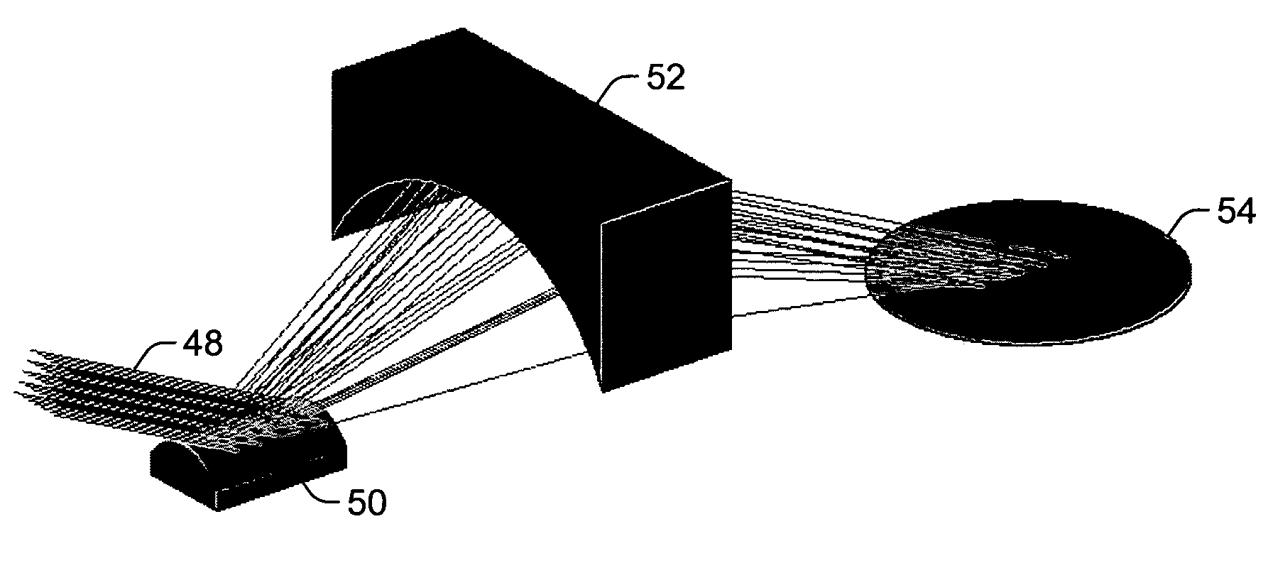
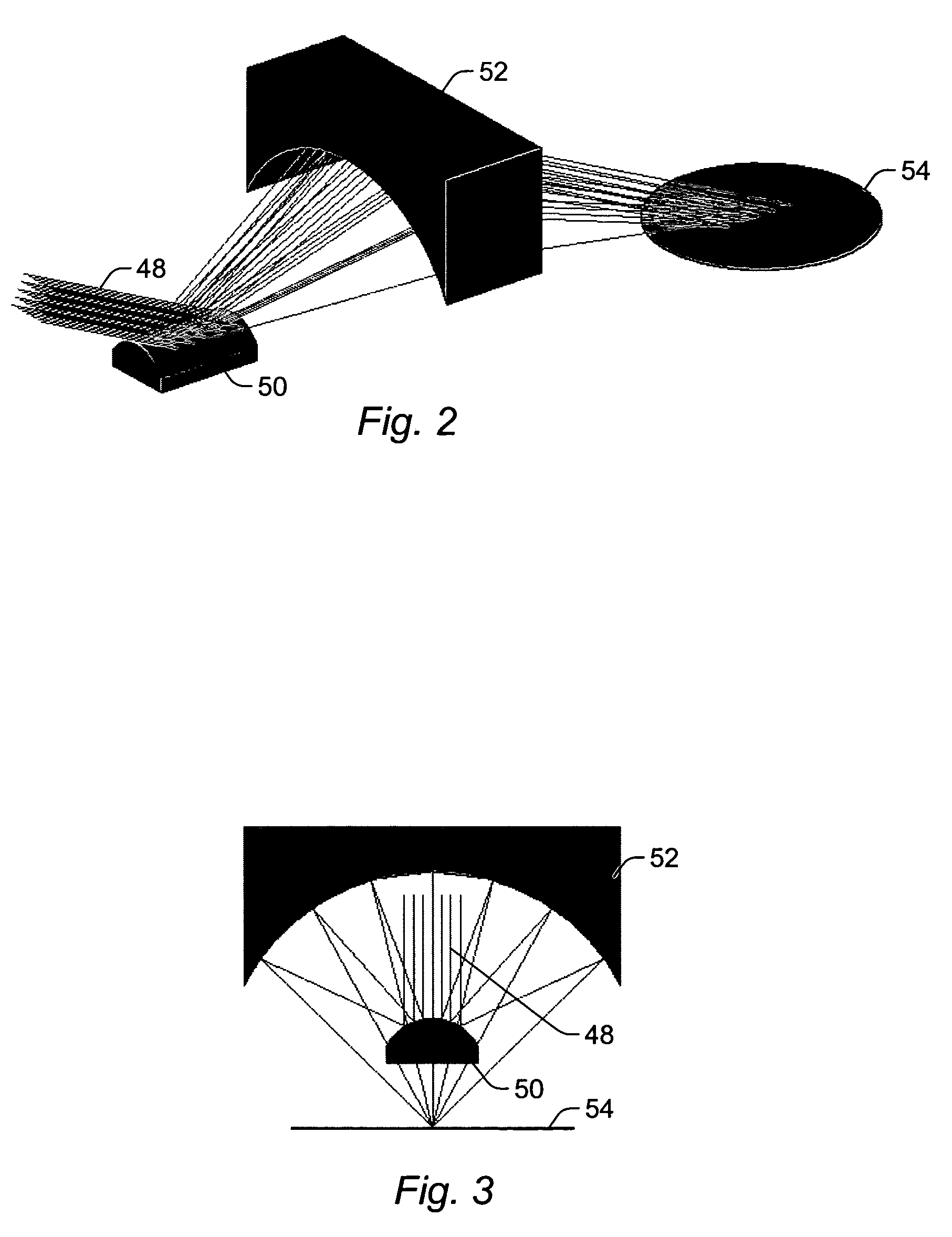
[0035]As used herein, the term “specimen” generally refers to a wafer or any other specimen that can be inspected using obliquely incident light.

[0036]As used herein, the term “wafer” generally refers to substrates formed of a semiconductor or non-semiconductor material. Examples of such a semiconductor or non-semiconductor material include, but are not limited to, mono crystalline silicon, gallium arsenide, and indium phosphide. Such substrates may be commonly found and / or processed in semiconductor fabrication facilities. A wafer may include one or more layers formed upon a substrate. For example, such layers may include, but are not limited to, a resist, a dielectric material, and a conductive material. Many different types of such layers are known in the art, and the term wafer as used herein is intended to encompass a wafer including all types of such layers.

[0037]One or more layers formed on a wafer may be patterned or unpatterned. For example, a wafer may include a plurality ...


PUM

PropertyMeasurementUnit
working distanceaaaaaaaaaa
wavelengthaaaaaaaaaa
angle of incidenceaaaaaaaaaa

Abstract

Systems configured to provide illumination of a specimen during inspection are provided. One system includes catoptric elements configured to direct light from a light source to a line across the specimen at an oblique angle of incidence. The catoptric elements include positive and negative elements configured such that pupil distortions of the positive and negative elements are substantially canceled. Another system includes a dioptric element and a catoptric element. The dioptric element and the catoptric element are configured to direct light from a light source to a line across the specimen at an oblique angle of incidence. The dioptric and catoptric elements are also configured such that pupil distortions of the dioptric and catoptric elements are substantially canceled.

Description

BACKGROUND OF THE INVENTION[0001]1. Field of the Invention[0002]This invention generally relates to systems configured to provide illumination of a specimen during inspection. Certain embodiments relate to a system that is configured to provide illumination of a specimen during inspection that includes elements configured such that pupil distortions of the elements substantially cancel.[0003]2. Description of the Related Art[0004]The following description and examples are not admitted to be prior art by virtue of their inclusion in this section.[0005]Fabricating semiconductor devices such as logic and memory devices typically includes processing a substrate such as a semiconductor wafer using a large number of semiconductor fabrication processes to form various features and multiple levels of the semiconductor devices. For example, lithography is a semiconductor fabrication process that involves transferring a pattern from a reticle to a resist arranged on a semiconductor wafer. Add...

Claims


Application Information

Patent Timeline
Patent Type & Authority Patents(United States)
IPC IPC(8): G02B17/00G01N21/00
CPCG01N21/8806G01N21/9501G02B17/0804G02B17/0852G01N2201/0636
Inventor JEONG, HWAN J.
Owner KLA TENCOR TECH CORP
Why Eureka
Try Eureka