Ferroelectric storage device

a storage device and ferroelectric technology, applied in the field of ferroelectric storage devices, can solve the problems of insufficient constraint of a variation of a characteristic, and achieve the effect of stable detection

Active Publication Date: 2007-04-03
FUJITSU SEMICON MEMORY SOLUTION LTD
View PDF5 Cites 6 Cited by
  • Summary
  • Abstract
  • Description
  • Claims
  • Application Information

AI Technical Summary

Benefits of technology

[0010]According to the ferroelectric storage device, the potential control circuit controls the potentials of the bit line and the reference bit line, whereby the potentials can be properly shared between the bit line capacitor and the ferroelectric capacitor. Therefore, the data outputted to the bit lines can be stably detected. Further, the timing control circuit that controls the detection timing for detecting the data on the bit lines is provided, whereby the data outputted to the bit lines can be detected at a proper timing.
[0011]Further, the invention may also be a ferroelectric storage device comprising ferroelectric capacitors each retaining complementary data, bit lines receiving respective outputs of pieces of complementary data from the ferroelectric capacitors, and a detection circuit detecting a potential difference between these pieces of complementary data before the two pieces of complementary data outputted to the bit lines are stabilized. According to the ferroelectric storage device, the potential difference between the pieces of complementary data is detected before both of the complementary data outputted to the bit lines are stabilized, and hence there increases a possibility enabling the detection of a much larger potential difference than in the case of detecting the potential difference between the pieces of complementary data after the both have been stabilized.

Problems solved by technology

Further, the ferroelectric capacitor has a problem that restraint of a variation of the characteristic is insufficient, and so on.

Method used


Image

  • Ferroelectric storage device
  • Ferroelectric storage device
  • Ferroelectric storage device

Examples


first embodiment

[0028]A first embodiment of the invention will hereinafter be explained with reference to the drawings in FIGS. 1 through 7 and FIGS. 11 through 14.

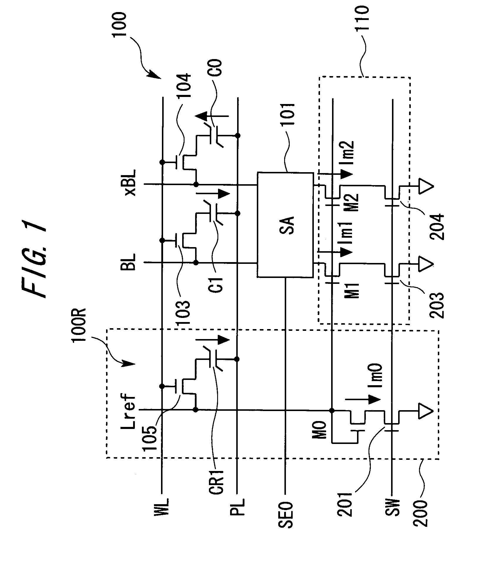
[0029]FIG. 11 is a circuit diagram showing an example of a configuration of the ferroelectric memory. This circuit includes ferroelectric capacitors C1 and C0 that store complementary data on each other, a bit line BL and a complementary bit line xBL that serve to input and output the data of the respective ferroelectric capacitors C1 and C0, an n-channel MOS (Metal-Oxide Semiconductor) field-effect transistor (FET) 103 that selectively connects the ferroelectric capacitor C1 and the bit line BL, an n-channel MOSFET 104 that selective connects the ferroelectric capacitor C0 and the complementary bit line xBL, a word line WL for controlling gate voltages of the n-channel MOSFETs 103 and 104, a plate line connected to a terminal on the opposite side to the n-channel MOSFET 103 (and 104) of the ferroelectric capacitor C1 (and C0), and a sen...

example

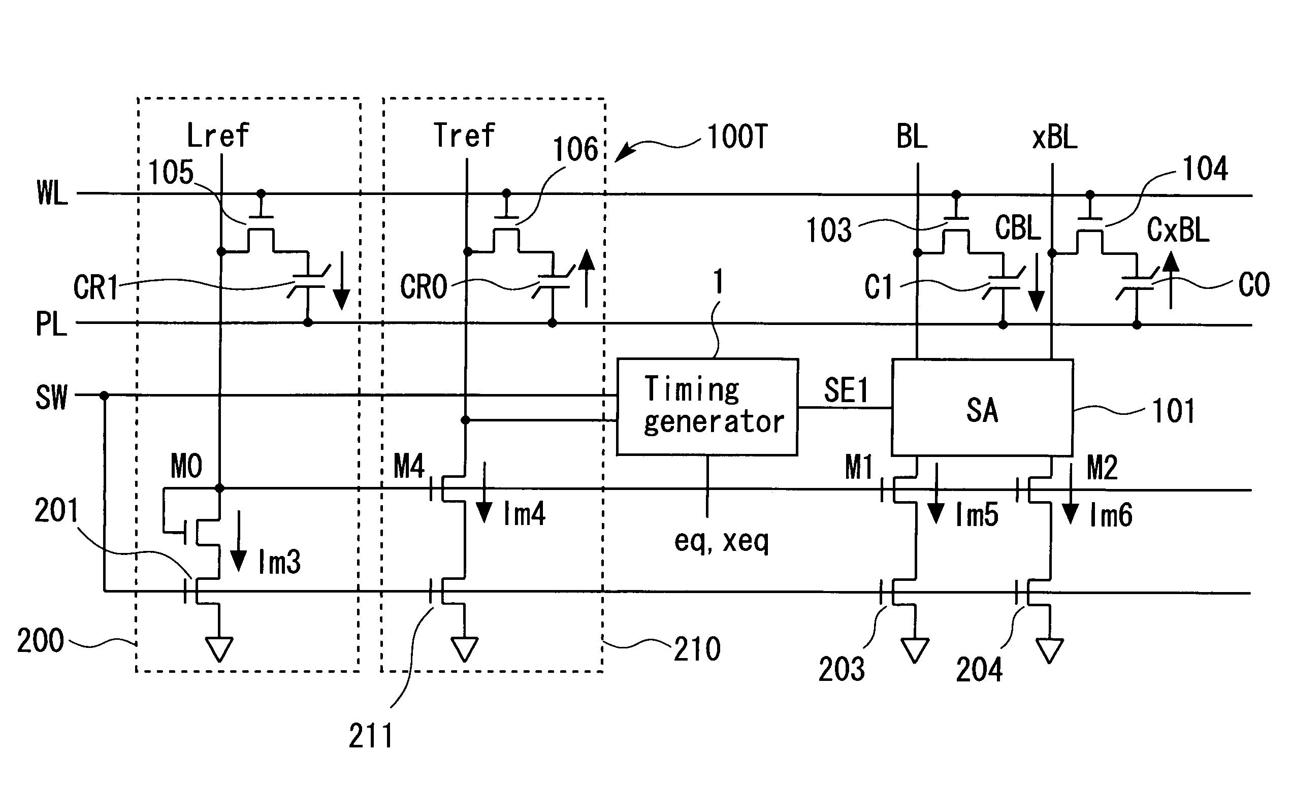
[0072]FIG. 4 shows a circuit configuration of the ferroelectric capacitor memory according to the first embodiment of the invention. The ferroelectric capacitor memory in FIG. 4 has further additions, to the basic circuit illustrated in FIG. 1, of a second reference circuit 210 and a timing generation circuit 1 (corresponding to a judging circuit according to the invention). The reference circuit 210 and the timing generation circuit 1 correspond to a timing control circuit according to the invention. In FIG. 4, the configuration excluding the second reference circuit 210 and the timing generation circuit 1 is the same as the basic circuit in FIG. 1. This being the case, the same components as those in FIG. 1 are marked with the same numerals and symbols, and their explanations are omitted.

[0073]As explained in FIG. 1, the reference circuit 200 supplies the voltage to the gates of the transistors M1 and M2. Namely, the reference circuit 200 controls the potentials of the bit line BL...

second embodiment

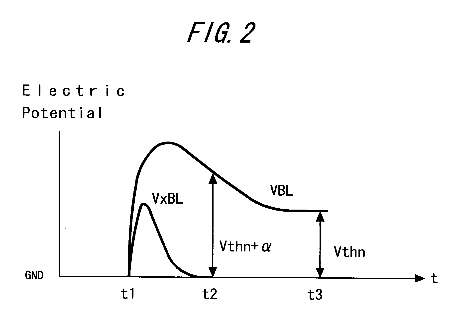
[0104]A second embodiment of the invention will be described with reference to the drawings in FIGS. 8 through 10. In the first embodiment, the timing for activating the sense amplifier 101 detecting the potential difference ΔVBL between the bit line BL and the complementary bit line xBL of the memory cell, is determined in a way that detects the change in potential of the complementary reference bit line Tref when reading from the reference ferroelectric capacitor CR0.

[0105]In the case of such a configuration, an advantage is that the sense amplifier 101 can be activated at the timing when the potential difference ΔVBL between the bit line BL and the complementary bit line xBL keeps a value larger than the threshold voltage Vth in the case of the basic circuit (FIG. 1) from the change in potential of the complementary reference bit line Tref. In such a configuration, however, the characteristic of the reference ferroelectric capacitor CR0 or CR1 deteriorates, the hysteresis is weak...


PUM


Abstract

A ferroelectric storage device includes a ferroelectric capacitor C1, a bit line BL, a first switching element 103 selectively connecting the ferroelectric capacitor C1 and the bit line BL, a first transistor 203 connected to the bit line BL and to a reference potential, a reference ferroelectric capacitor CR1, a reference bit line Lref, a reference switching element 105 selectively connecting the reference ferroelectric capacitor CR1 and the reference bit line Lref, a second transistor 201 connected to the reference bit line Lref and to the reference potential, potential control circuits 110 and 200 controlling a potential of the bit line BL and a potential of the reference bit line Lref, and a timing control circuit 210 controlling a detection timing for detecting data on the bit line.

Description

CROSS-REFERENCE TO RELATED APPLICATIONS[0001]This application is based upon and claims the benefit of priority from the prior Japanese Patent Application No. 2005-197945, filed in Jul. 6, 2005, the entire contents of which are incorporated herein by reference.BACKGROUND OF THE INVENTION[0002]The present invention relates to a ferroelectric storage device.[0003]A ferroelectric capacitor, though nonvolatile, has a characteristic capable of reading and writing data at a high speed. The ferroelectric capacitor is utilized for a ferroelectric memory (FeRAM (Ferroelectric Random Access Memory)) by making the use of this characteristic.[0004]A readout characteristic of a cell potential of the ferroelectric memory, as in the case of a DRAM (Dynamic RAM), depends on a ratio of a ferroelectric capacitor that are provided in the cell to a bit line capacitor. With the high integration of the memory, as a memory area is reduced, a capacitor of the bit line decreases. As a result, in voltages app...

Claims


Application Information

Patent Timeline
Patent Type & Authority Patents(United States)
IPC IPC(8): G11C11/22
CPCG11C11/22G11C5/063G11C5/14G11C7/12G11C7/22G11C11/221G11C11/2273G11C11/2297
Inventor YOSHIOKA, HIROSHI
Owner FUJITSU SEMICON MEMORY SOLUTION LTD
Why Eureka
Try Eureka