Memory unit and semiconductor device

a memory unit and semiconductor technology, applied in semiconductor devices, digital storage, instruments, etc., can solve the problems of difficult to obtain uniform characteristics not only between chips but also in chips, and the like, and achieve the effect of simplifying the configuration of the memory

Active Publication Date: 2007-04-03
SEMICON ENERGY LAB CO LTD
View PDF7 Cites 32 Cited by
  • Summary
  • Abstract
  • Description
  • Claims
  • Application Information

AI Technical Summary

Benefits of technology

[0012]In view of the foregoing, it is the primary object of the present invention to provide a memory unit that is capable of operating in a desired operation condition while suppressing the power consumption, and a semiconductor device using the memory unit.
[0023]With the above-mentioned configuration, it is possible to suppress variations in characteristics between memory cells in a memory or between memories on different chips. Further, according to the present invention power consumption can be suppressed and a potential can be optimized in accordance with the operation condition. It is also possible to suppress the deterioration of characteristics of a switching element or a memory element caused by supplying too high or too low potential.
[0024]The memory of the present invention comprises a selection circuit, a power source circuit and the like as hardware for the potential optimization, which is performed by software with a CPU. In the case where a series of operations for optimization is not controlled by a program but by dedicated hardware, large-scale and complex hardware is necessarily provided in the memory. In this case, it is difficult to reduce the size of a semiconductor device and the power consumption as the function of potential optimization is provided. Therefore, it is not realistic. In addition, since different hardware is required to be provided in accordance with user needs, it has poor versatility. In the present invention, by utilizing hardware partially and controlling the optimization operation by software, the configuration of a memory can be simplified, the optimization corresponding to the operation condition can be performed much more freely, and the power consumption can be suppressed as compared with the case where the optimization is performed only by hardware.
[0026]The memory of the present invention comprises a selection circuit and a power source circuit as hardware for the correction, and the correction of characteristics of a cell array using the selection circuit and the power source circuit is performed by controlling the selection circuit and the power source circuit by software. By utilizing hardware partially and performing the correction by software as described above, optimization corresponding to the operation condition can be performed more freely and the configuration of the memory can be simplified as compared with the case where the correction is performed only by hardware.

Problems solved by technology

In addition, the characteristics may vary with time even in the same chip due to the heat generated by an integrated circuit and the like or to deterioration with the passage of driving time.
On the other hand, as for a memory formed by using a thin semiconductor film, characteristics of a semiconductor elements used as switching elements vary more often than that using a single crystalline semiconductor substrate, and the uniformity of the characteristics is difficult to obtain not only between chips but also in a chip.
However, variations in characteristics of the mobility, the threshold voltage, and the like tend to occur due to defects in a grain boundary.

Method used


Image

  • Memory unit and semiconductor device
  • Memory unit and semiconductor device
  • Memory unit and semiconductor device

Examples


embodiment mode 1

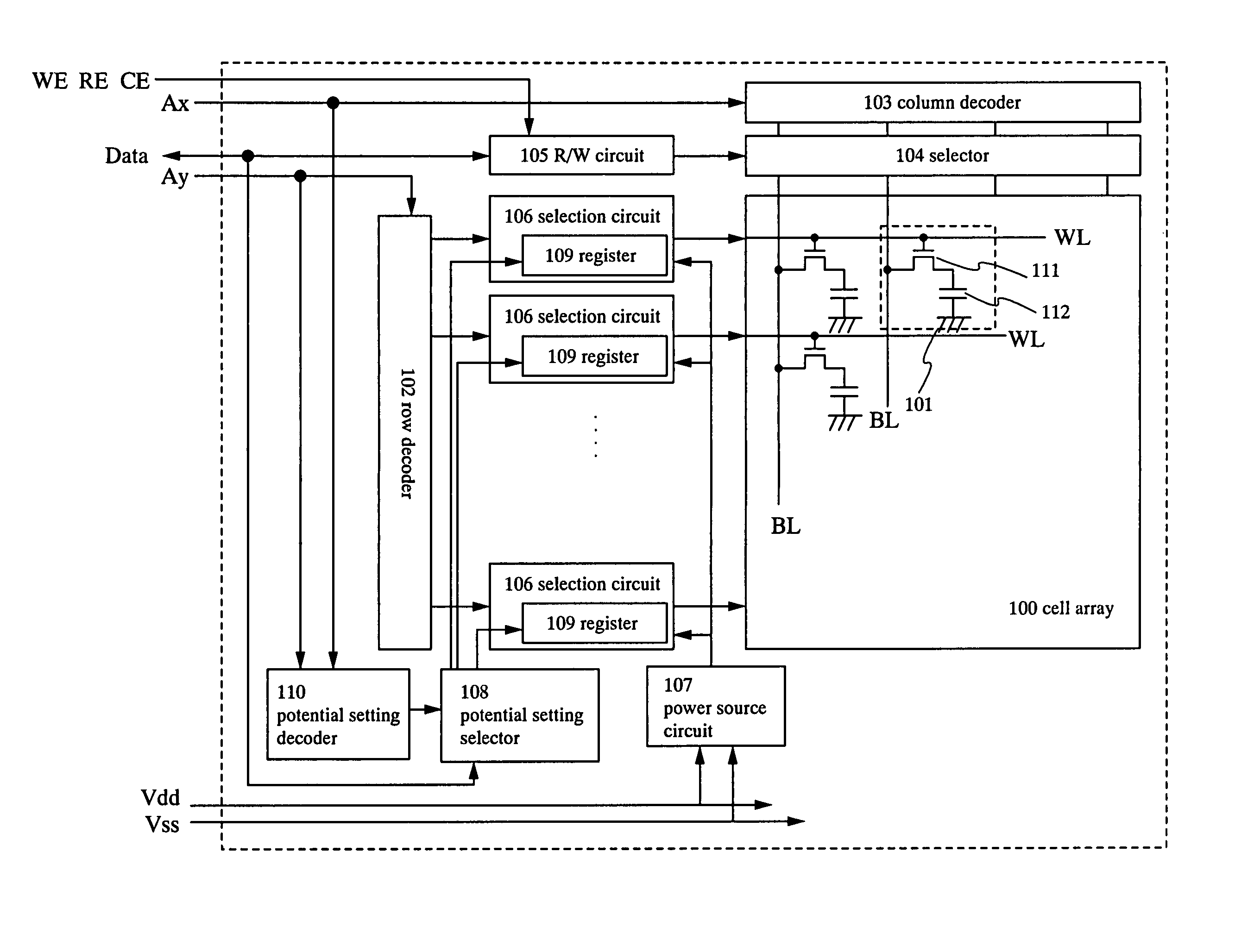
[0037]A configuration of a memory according to the present invention will be explained using FIG. 1. A memory shown in FIG. 1 is a DRAM and explained is one embodiment mode in which a potential of a word line is optimized.

[0038]In the memory in FIG. 1, reference numeral 100 denotes a cell array in which a plurality of memory cells 101 are arranged in matrix. Each memory cell 101 comprises a word line WL, a bit line BL, a transistor (pass transistor) 111 that serves as a switching element, and a capacitor 112. Reference numeral 102 denotes a row decoder, 103 denotes a column decoder, 104 denotes a selector, 105 denotes a R / W circuit, 106 denotes a selection circuit, and 107 denotes a power source circuit. The selection circuit 106 comprises a register 109 which serves as a memory circuit. The row decoder 102, the column decoder 103, the selector 104, and the R / W circuit 105 correspond to driver circuits for controlling the operation of the memory cell 101. Reference numeral 108 denot...

embodiment mode 2

[0057]Explained in this embodiment mode are a DRAM of gain cell type, which is one of the memories of the present invention, and a method for setting a potential supplied to a memory cell of the DRAM.

[0058]FIG. 4 shows a configuration of a memory according to this embodiment mode. Reference numeral 300 denotes one of memory cells provided in a cell array. Only one memory cell 300 is shown in FIG. 4, however, a plurality of memory cells 300 are provided in matrix in a cell array practically. In this embodiment mode, the memory cell 300 comprises a bit line BL, two word lines WLb and WLf, a source line SL, and a TFT 302 which serves as a memory element and a switching element.

[0059]Reference numeral 303 denotes a row decoder, 304a and 304b denote selection circuits, 305 denotes a potential setting selector, 306 denotes a potential setting decoder, and 307 denotes a power source circuit. The selection circuits 304a and 304b comprise registers 308a and 308b for storing selection data, s...

embodiment 1

[0101]Explained in this embodiment is a case where a plurality of potentials to be supplied to a selection circuit from a power source circuit are optimized as well as a potential to be supplied to a memory cell.

[0102]FIG. 8 shows a configuration of a memory according to this embodiment. FIG. 8 is the memory based on FIG. 1 in which a function for optimizing a plurality of potentials to be supplied to a selection circuit from a power source circuit is additionally provided. The components already shown in FIG. 1 are denoted by the same reference numerals in FIG. 8. The memory shown in FIG. 8 is a DRAM, though the memory according to this embodiment is not limited to this. In addition, an embodiment mode of optimizing a potential of a word line is shown in FIG. 8 as well as in FIG. 1, however, the memory according to this embodiment is not limited to this.

[0103]In the memory shown in FIG. 8, a power source circuit 107 includes a register for selecting a potential to be supplied to a ...


PUM


Abstract

A memory unit that is capable of operating in a desired operation condition with less power consumption, and a semiconductor device using the memory unit. The memory circuit comprises a cell array in which a plurality of memory cells is arranged, a driver circuit, a plurality of selection circuits each of which includes a memory circuit, and a power source circuit. A plurality of potentials is supplied to each of plurality of selection circuits from the power source circuit, each of plurality of selection circuits selects a potential among the plurality of potentials in accordance with data stored in each memory circuit, and the selected potential is supplied to a memory cell corresponding to each of the plurality of selection circuits among the plurality of memory cells by a signal output from the driver circuit.

Description

BACKGROUND OF THE INVENTION[0001]1. Field of the Invention[0002]The present invention relates to a memory unit having a characteristic correcting function and to a semiconductor device to which the memory unit is mounted.[0003]2. Description of the Related Art[0004]A semiconductor memory (abbreviated to a memory, hereinafter) is a typical memory unit which is configured mainly by a MOS transistor, and has advantages in that it is capable of operating at a higher speed than a magnetic recording medium, does not require a mechanical driving part, few breakdowns occur, the lifetime is long and the like. Included in the typical memories are a DRAM (Dynamic Random Access Memory) and an SRAM which are volatile memories, and a masked ROM, an EPROM, an EEPROM, a flash memory, and a ferroelectric memory which are nonvolatile memories and the like. These memories each of which is formed using a single crystalline semiconductor substrate have already been put into practice and abundantly avail...

Claims


Application Information

Patent Timeline
Patent Type & Authority Patents(United States)
IPC IPC(8): G11C5/14G11C11/4074G11C11/408H01L21/8242H01L27/105H01L27/108H01L27/12H01L29/786
CPCG11C11/4074G11C11/4085H01L27/105H01L27/10891H01L27/10897H01L29/78648H01L29/78672H10B12/488H10B12/50
Inventor KATO, KIYOSHI
Owner SEMICON ENERGY LAB CO LTD
Why Eureka
Try Eureka