Method for the implementation of electronic components in via-holes of a multi-layer multi-chip module

a multi-chip module and electronic component technology, applied in the direction of resistor housing/enclosement/embedding, resistive material coating, printed element electric connection formation, etc., can solve the problem of reducing the signal to noise ratio, unable to obtain resistors within narrow tolerances, and attendant heating

Inactive Publication Date: 2007-04-10
SCHUSTER ISRAEL
View PDF17 Cites 4 Cited by
  • Summary
  • Abstract
  • Description
  • Claims
  • Application Information

AI Technical Summary

Problems solved by technology

“Because the photopolymerization process may form lines having sides that are not entirely uniform or smooth, it may be difficult to obtain resistors within narrow tolerances without further processing.” In applications where precise resistance is necessary, the resistor lines are made wider than necessary and, after curing, each of the resistors is measured and trimmed with a laser to increase the resistance.
Thus, creating a multi-layer system results in conducting lines no shorter than the original single layer MCM with the attendant heating, energy loss, and reduced signal to noise ratio.
Most of the existing methods of producing passive elements on substrate surfaces require multi-step, relatively complex, manufacturing processes and relatively large volumes of expensive substrate material.
Also,

Method used


Image

  • Method for the implementation of electronic components in via-holes of a multi-layer multi-chip module
  • Method for the implementation of electronic components in via-holes of a multi-layer multi-chip module
  • Method for the implementation of electronic components in via-holes of a multi-layer multi-chip module

Examples


Embodiment Construction

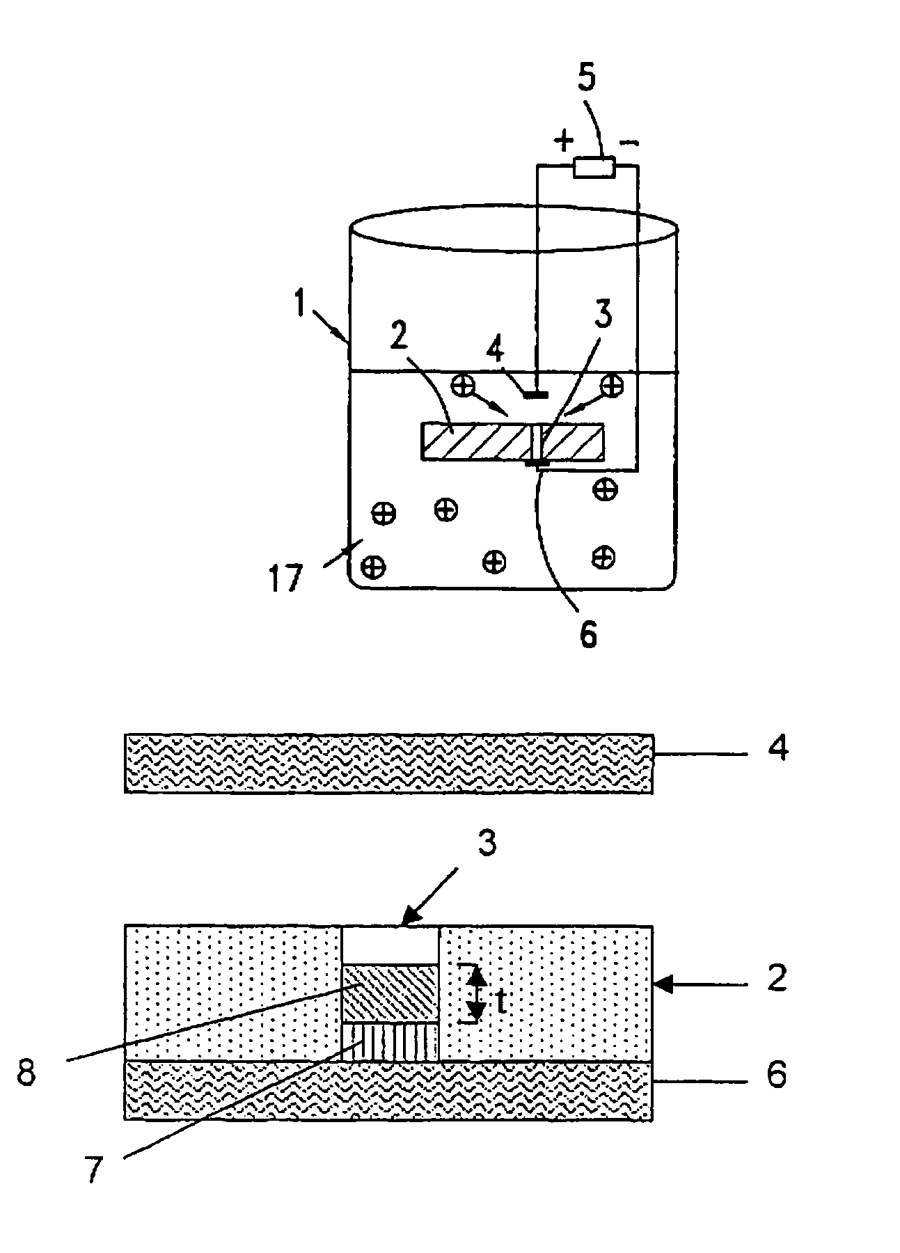
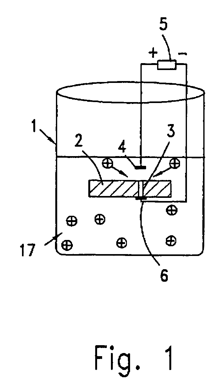
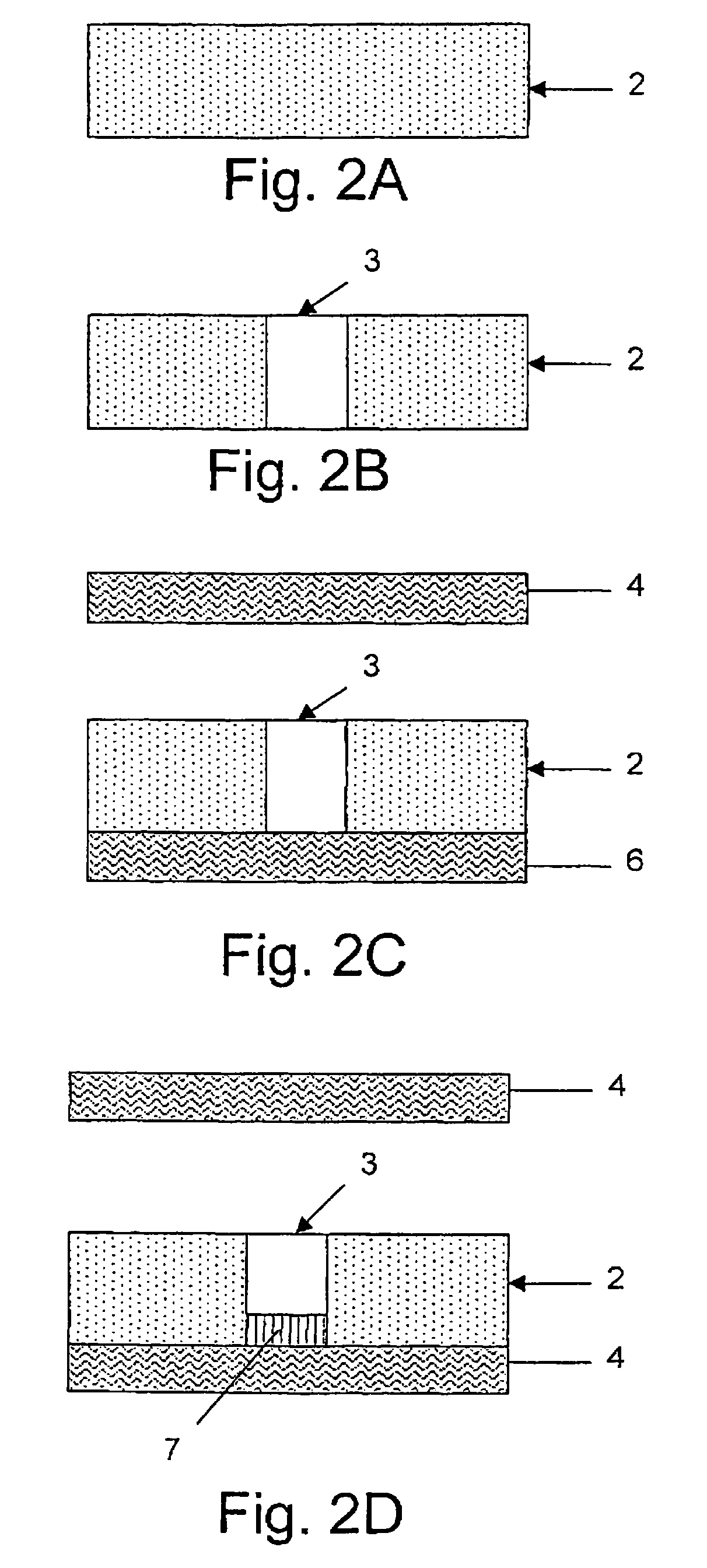
[0095]An electrophoretic deposition (EPD) cell 1 is shown schematically in FIG. 1. The cell 1 consists of a container with an electric circuit consisting of an “upper” positive electrode 4 connected through a DC power supply 5 to a “lower” negative electrode 6. The substrate and electrodes are suspended in a liquid suspension 17.

[0096]The suspension consists of particles of the material that has been chosen for the manufacture of the electrical component to which positive electrical charges have been attached by adsorption of ions. The particles are suspended in either water or any other suitable liquid, such as alcohol, depending upon the properties of the powder to be placed in suspension and the type of substrate.

[0097]As mentioned above, the particles of the suspension are chosen according to the type of passive component that should be formed and the desired values of the electrical properties of said component. Conductors are produced from metals, including gold, silver, coppe...


PUM

PropertyMeasurementUnit
Volumeaaaaaaaaaa
Electrical conductoraaaaaaaaaa

Abstract

The substrate (2) containing the via-hole (3) is inserted into an electrophoretic cell (1) and an electrode (6) (the “first electrode”) is placed on top of a first orifice of the via-hole(s) (3), to be implemented with electrical component(s), so that the electrode (6) totally covers the first orifice. Electrically charged either conductive and/or non-conductive particles are provided by immersing the volume of the via-hole(s) (3) in a conductive medium (17) consisting of the electrically charged particles. An electric field is created between the first electrode (6) and a second electrode (4) through the via-hole(s) (3) and the conductive medium (17) and the electrically charged particles are precipitated on the inner surface of the first electrode (6) that is directed to the second orifice of the via-hole(s) (3), until a desired portion of the volume of the via-hole(s) (3) is filled with a first layer of the charged particles having a desired thickness. More layers may be created by repeating this process using additional electophoretic cell(s), until remaining portion of the volume of the via-hole(s) (3) is filled with the additional charged particles.

Description

CROSS-REFERENCE TO RELATED APPLICATION[0001]This application is the U.S. National Phase under 35 U.S.C. 371 of International Application PCT / IL01 / 00991, filed Oct. 25, 2002, which claims priority to Israeli Patent Application No. 141118, filed Jan. 25, 2001.FIELD OF THE INVENTION[0002]The present invention relates to the field of integrated multi-layer multi-chip modules (MCMs), to the manufacture of integrated multi-layer MCMs, and specifically to the manufacture of integrated multi-layer MCMs in which electrical components are produced in the via-holes that provide the electrical continuity between the layers.BACKGROUND OF THE INVENTION[0003]Many different types of substrate serve as the supporting and interconnecting substrate for electronic components. Resistors, capacitors, inductors, and many other types of electronic component are mounted on the substrate in a predetermined manner and electrically connected together by a metallic conducting pattern that is deposited on its su...

Claims


Application Information

Patent Timeline
IPC IPC(8): H01C17/00H01L21/48H01L23/538H01L23/58H01L23/64H05K1/03H05K1/16H05K3/40H05K3/46
CPCH01L21/486H01L23/5384H01L23/58H01L23/647H05K1/16H05K3/4061H01L23/5383Y10T29/49099H01L2924/09701H01L2924/12044H05K1/0306H05K1/162H05K1/165H05K1/167H05K3/4611H05K3/4629H05K2201/0209H05K2203/135H01L2224/32225H01L2924/15192H01L2924/19105Y10T29/49082Y10T29/49089Y10T29/49101
Inventor SCHUSTER, ISRAEL
Owner SCHUSTER ISRAEL
Why Eureka
Try Eureka