Method for manufacturing ultrafine carbon fiber and field emission element

a manufacturing method and technology for carbon fiber, applied in the manufacture of electrode systems, electric discharge tubes/lamps, nanoinformatics, etc., can solve the problems of large variation in diameter, difficult to control the diameter of cnt, and difficult to separate the diameter and length of ultrafine carbon fiber in the conventional manufacturing method, etc., to achieve high reliability and high productivity

Active Publication Date: 2007-04-10
SEMICON ENERGY LAB CO LTD
View PDF17 Cites 38 Cited by
  • Summary
  • Abstract
  • Description
  • Claims
  • Application Information

AI Technical Summary

Benefits of technology

[0025]It is possible to control a diameter of an ultrafine carbon fiber according to a method for manufacturing an ultrafine carbon fiber of the invention, so that an ultrafine carbon fiber having a uniform diameter can be formed. In addition, a field emission element that has an ultrafine carbon fiber whose diameter is uniform as an electron emission portion can be formed. Furthermore, density of an electron emission portion of a field emission element can be also controlled. Accordingly, it is possible to uniformly discharge an emission current per pixel; therefore, a FED that enabled a display without variation can be formed.
[0026]In addition, an ultrafine carbon fiber manufactured according to the invention has an uniform diameter; therefore, a probe of a Scanning Probe Microscope (SPM), a FET, a negative electrode material of a lithium battery, a gas occluding substance, or the like having high reliability can be manufactured.
[0027]In the invention, it is possible to manufacture a field emission element by using a large-sized substrate, which is suitable for a mass production process. Accordingly, an ultrafine carbon fiber, a semiconductor device, and a display device using an ultrafine carbon fiber can be manufactured by achieving high productivity.

Problems solved by technology

However, it is difficult to control separately a diameter and a length of an ultrafine carbon fiber in the conventional manufacturing method, and has a problem of large variation in a diameter.
In Reference 2, a CNT is formed using a metal dot as a catalyst; however, a step of forming a metal film of from several nm to several ten nm is complicated, that is, it is difficult to control a diameter of a CNT, which is problematic.

Method used


Image

  • Method for manufacturing ultrafine carbon fiber and field emission element
  • Method for manufacturing ultrafine carbon fiber and field emission element
  • Method for manufacturing ultrafine carbon fiber and field emission element

Examples


embodiment 1

(Embodiment 1)

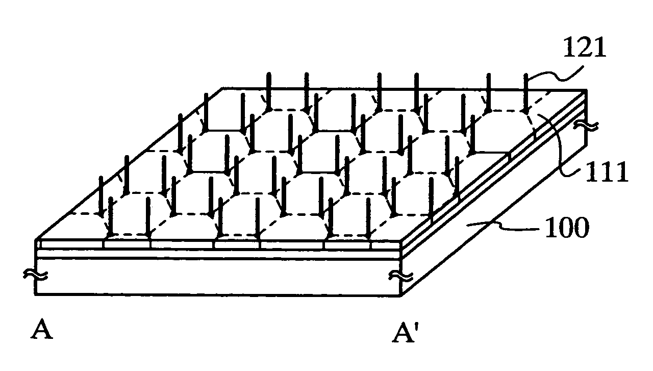
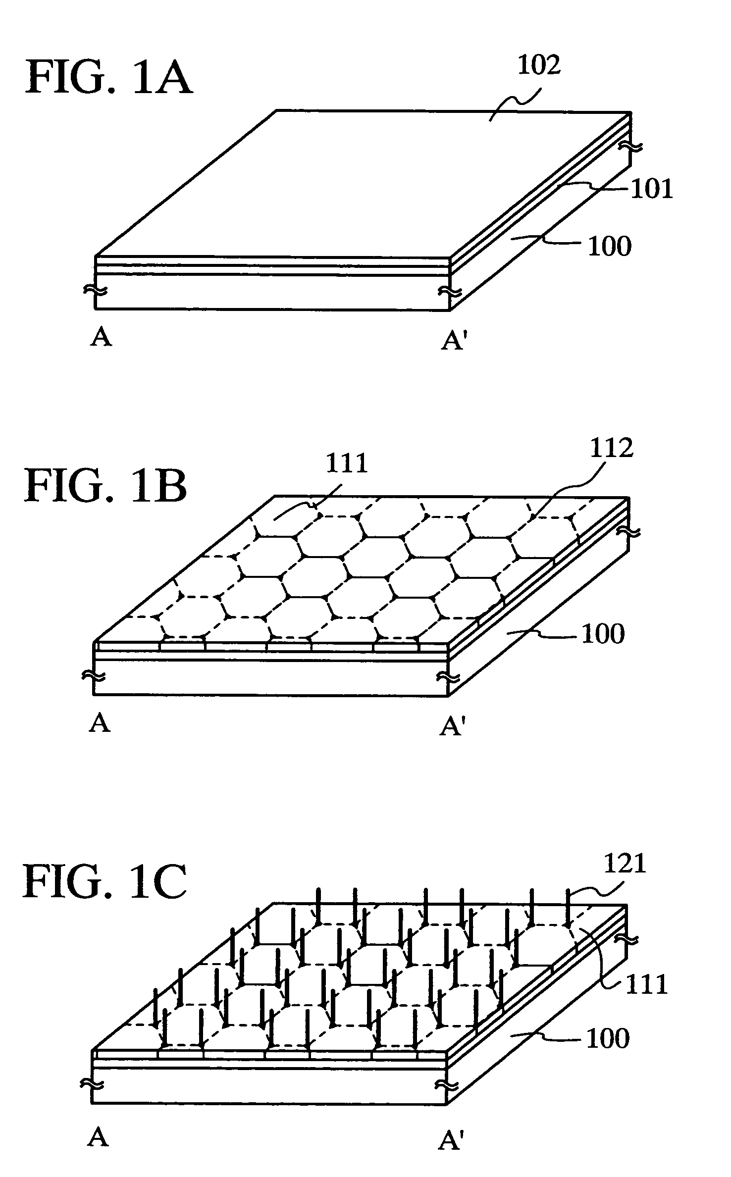
[0042]A method for manufacturing an ultrafine carbon fiber is described with reference to FIGS. 1A to 1C and 3A to 3C. FIGS. 1A to 1C are perspective views of substrate over which an amorphous semiconductor film and a crystalline semiconductor film are formed. FIGS. 3A to 3C are cross-sectional views taken along lines A–A′ in FIGS. 1A to 1C.

[0043]As shown in FIGS. 1A and 3A, an amorphous semiconductor film 102 is formed over a substrate 100 by interposing a first insulating film 101 therebetween.

[0044]The first insulating film 101 is formed of a film mainly containing silicon and oxygen (a silicon oxide film, a silicon nitride oxide film, a silicon oxynitride film, and the like) by a known method (CVD (Chemical Vapor Deposition), PVD (Physical Vapor Deposition), or the like). The first insulating film 101 can prevent a trace of alkali metal such as sodium (Na) contained in a glass substrate from dispersing.

[0045]The amorphous semiconductor film 102 is formed on the fir...

embodiment 2

(Embodiment 2)

[0051]Next, a method for manufacturing an ultrafine carbon fiber of the present invention, which is different from the above, is described with reference to FIGS. 1A to 1C and 4A to 4D.

[0052]As well as FIGS. 3A to 3C, FIGS. 4A to 4D are cross-sectional views taken along lines A–A′ in FIGS. 1A to 1C. As well as Embodiment 1, a first insulating film 101 and an amorphous semiconductor film 102 are sequentially formed over a substrate 100. Then, this amorphous semiconductor film 102 is crystallized. In this embodiment, laser crystallization is used for a crystallization method. The amorphous semiconductor film 102 is irradiated with laser light 104 using a gas laser oscillator, a solid laser oscillator, or a metal oscillator to form a crystalline semiconductor film 131. Continuous-wave or pulsed laser light can be used for the laser light 104 at this time.

[0053]As shown in FIG. 4B, a thin film 132 having a metal element is formed on the crystalline semiconductor film 131 b...

embodiment 3

(Embodiment 3)

[0058]Next, a method for manufacturing an ultrafine carbon fiber of the present invention, which is different from the above, is described.

[0059]As well as FIGS. 3A to 3C and 4A to 4D, FIGS. 5A to 5C are cross-sectional views taken along lines A–A′ in FIGS. 1A to 1C. As well as Embodiment 1, a first insulating film 101 and an amorphous semiconductor film 102 are sequentially formed over a substrate 100.

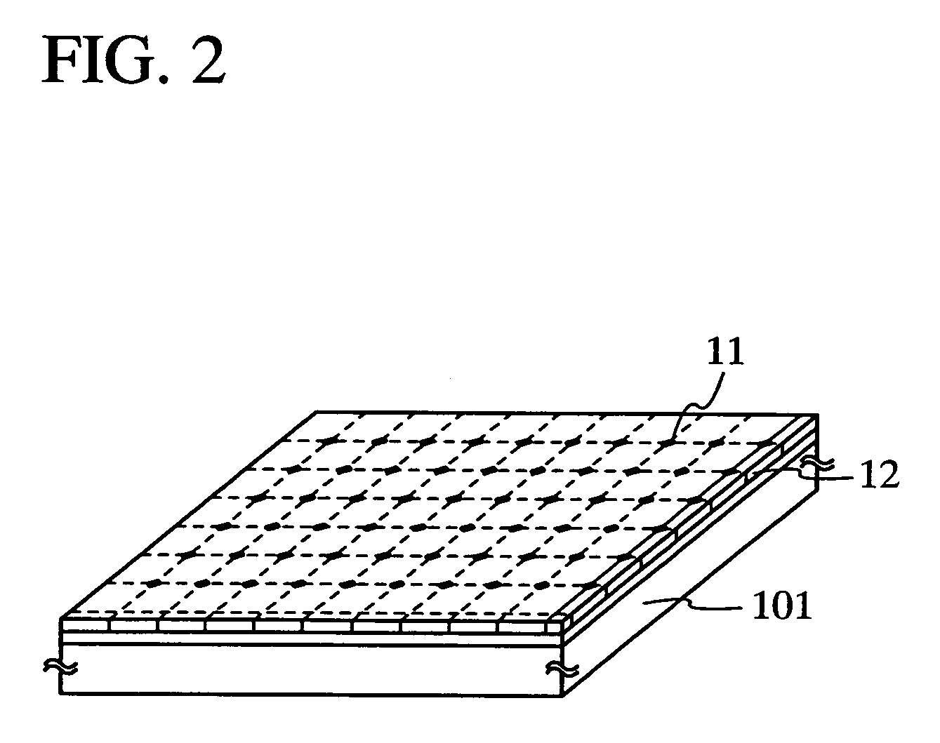
[0060]Next, as shown in FIG. 5A, a solution 103 containing from 1 ppm to 1000 ppm of a metal element is applied on the surface of the amorphous semiconductor film 102. Nickel (Ni), iron (Fe), cobalt (Co), platinum (Pt), titanium (Ti), palladium (Pd), or the like can be applied to the metal element.

[0061]Then, the amorphous semiconductor film 102 is crystallized. Here, laser crystallization is used for a crystallization method. The amorphous semiconductor film 102 is irradiated with laser light 104 using a gas laser oscillator, a solid laser oscillator, or a metal oscilla...


PUM

PropertyMeasurementUnit
lengthaaaaaaaaaa
lengthaaaaaaaaaa
lengthaaaaaaaaaa

Abstract

A method for manufacturing an ultrafine carbon fiber of the present invention has several steps as follows. In the first step, a semiconductor film is formed over a surface having insulative. In the second step, a first treatment is performed so that a metal element or a silicide of the metal element is segregated on a crystal grain boundary of the semiconductor film after adding the metal element in the semiconductor film. In the third step, a second treatment is performed so that an ultrafine carbon fiber on the surface of the metal element or the silicide of the metal element is formed.

Description

BACKGROUND OF THE INVENTION[0001]1. Field of the Invention[0002]The present invention relates to a method for manufacturing an ultrafine carbon fiber such as a graphite nanofiber, a carbon nanofiber, a carbon nanotube, tubular graphite, a carbon nanocone having a thin and sharp edge, corn shape graphite, or the like and a field emission element having the ultrafine carbon fiber.[0003]2. Description of the Related Art[0004]In recent years, an ultrafine carbon fiber is expected to be applied to various devices. Accordingly, various methods for manufacturing an ultrafine carbon fiber are examined.[0005]An arc discharge method, laser vaporization, CVD (Chemical vapor deposition), or the like is used for a typical manufacturing method of an ultrafine carbon fiber (Reference 1).[0006]There are an ultrafine carbon fiber such as a carbon nanotube (hereinafter, referred to as a CNT), a carbon nanofiber, a graphite nanofiber, tubular graphite, a carbon nanocone having a thin and sharp edge, o...

Claims


Application Information

Patent Timeline
Patent Type & Authority Patents(United States)
IPC IPC(8): H01J9/04C01B31/02C01B31/04D01F9/127H01J9/02H01J9/12H01J9/14
CPCB82Y10/00B82Y30/00B82Y40/00C01B31/0233C01B31/0293D01F9/127H01J9/025H01J2201/30469C01B32/162C01B32/18
Inventor OHNUMA, HIDETO
Owner SEMICON ENERGY LAB CO LTD
Why Eureka
Try Eureka