Semiconductor memory and method for operating the same

a technology of semiconductors and memory, applied in the field of semiconductor memory, can solve the problems of data loss, large power consumption during a standby period, and difficulty in operating the system in the manner, and achieve the effects of reducing chip size, eliminating defects, and easy operation of error correction circuits

Inactive Publication Date: 2007-04-10
SOCIONEXT INC
View PDF14 Cites 82 Cited by
  • Summary
  • Abstract
  • Description
  • Claims
  • Application Information

AI Technical Summary

Benefits of technology

[0011]Accordingly, it is an object of the invention to provide a pseudo SRAM capable of hiding a refresh operation without extending an access cycle time and capable of reducing power consumption during a standby period.

Problems solved by technology

However, since the pseudo SRAM stores data with charges accumulated in a capacitor of the memory cell, data might be lost due to charge leakage and so on.
For this reason, the refresh operation may conflict with an access operation.
Further, since the pseudo SRAM requires the refresh operation, its power consumption during a standby period is large, as compared with an SRAM whose memory cell includes a latch.
As a result, it is difficult to operate the system in the manner where the SRAM embedded in the system may be simply replaced with the pseudo SRAM, for example, for the sake of cost reduction.

Method used


Image

  • Semiconductor memory and method for operating the same
  • Semiconductor memory and method for operating the same
  • Semiconductor memory and method for operating the same

Examples


first embodiment

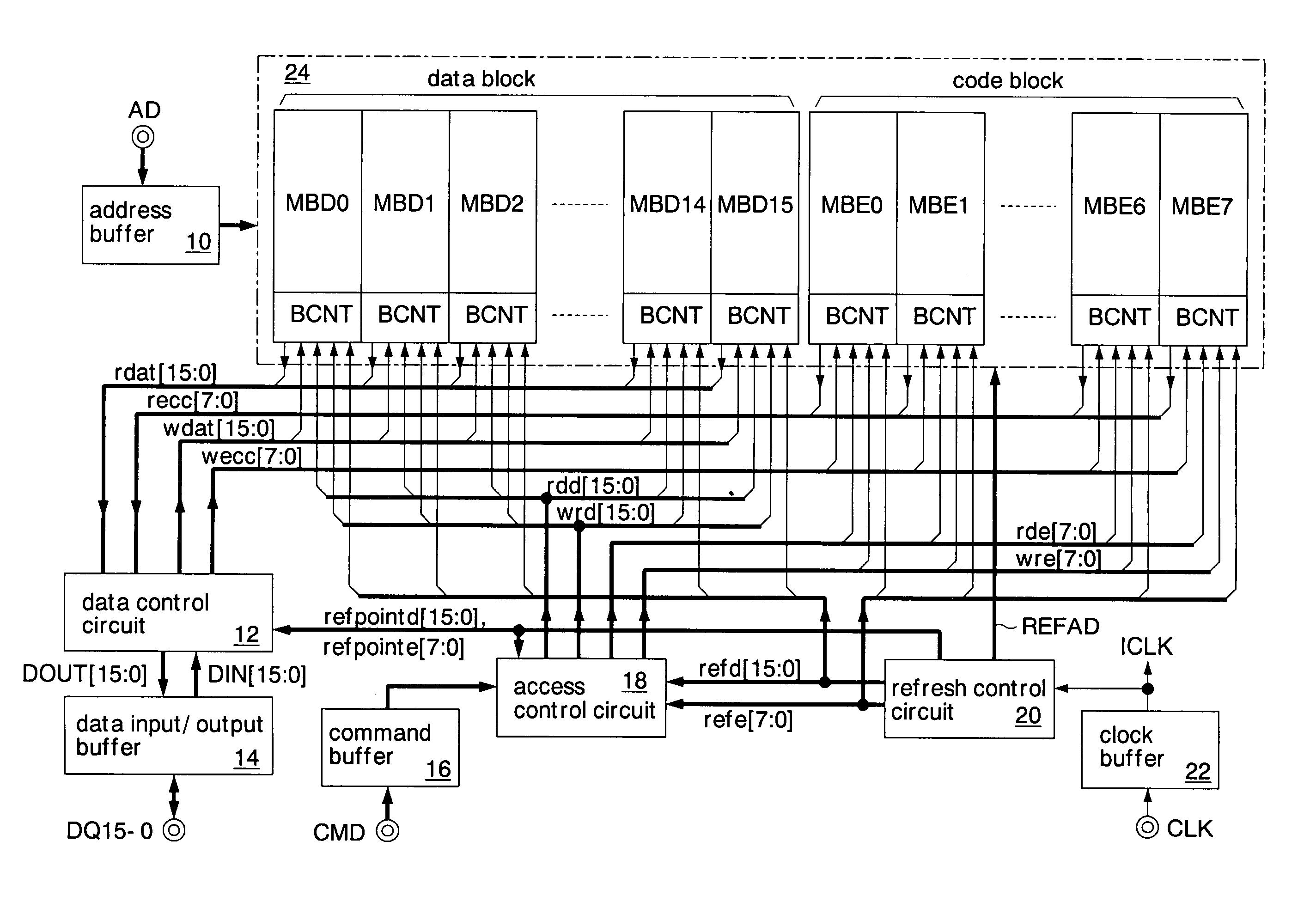
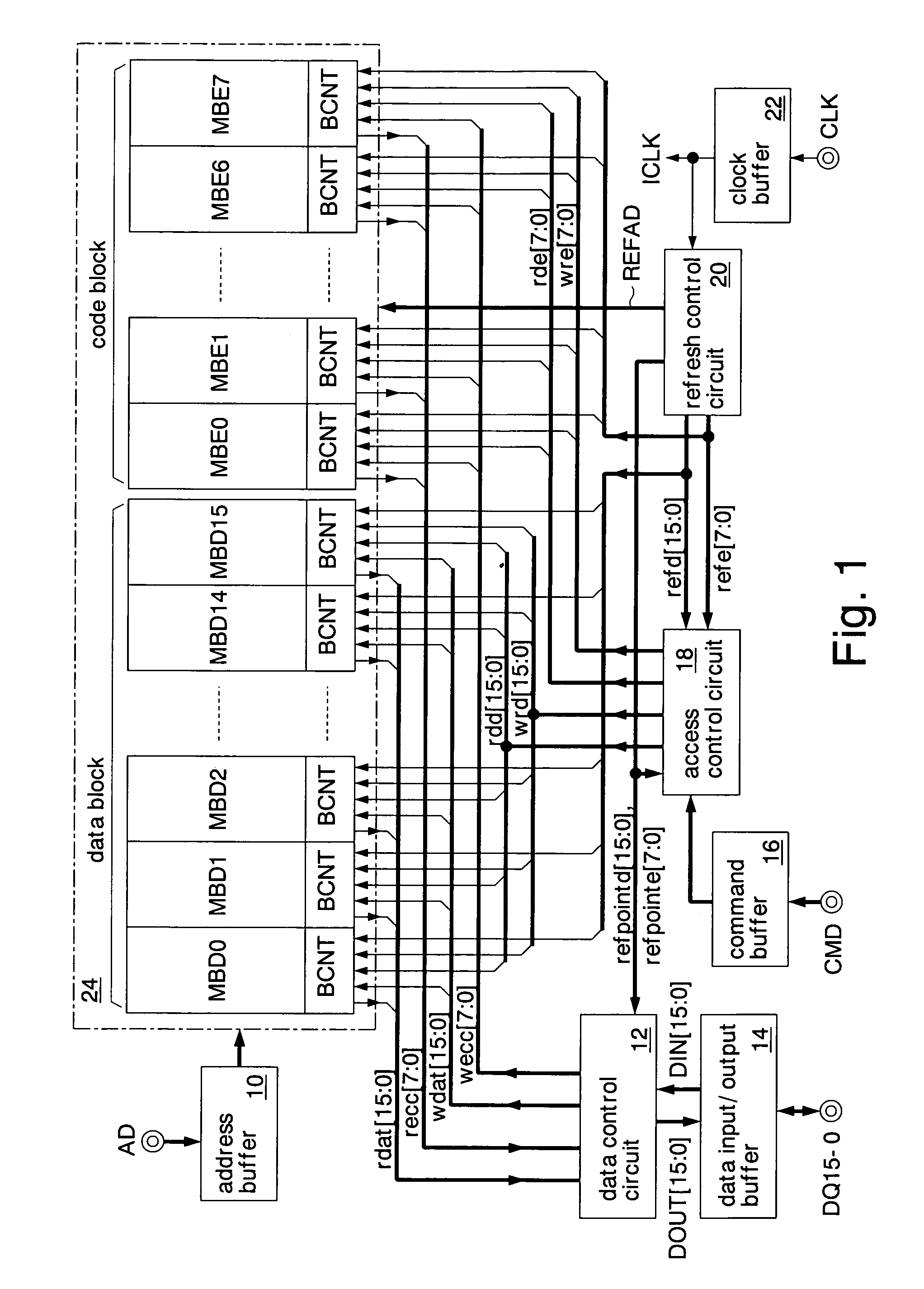
[0054]FIG. 1 shows a semiconductor memory according to the invention. The semiconductor memory is formed on a silicon substrate as a synchronous pseudo SRAM in a clock synchronous type using a CMOS process.

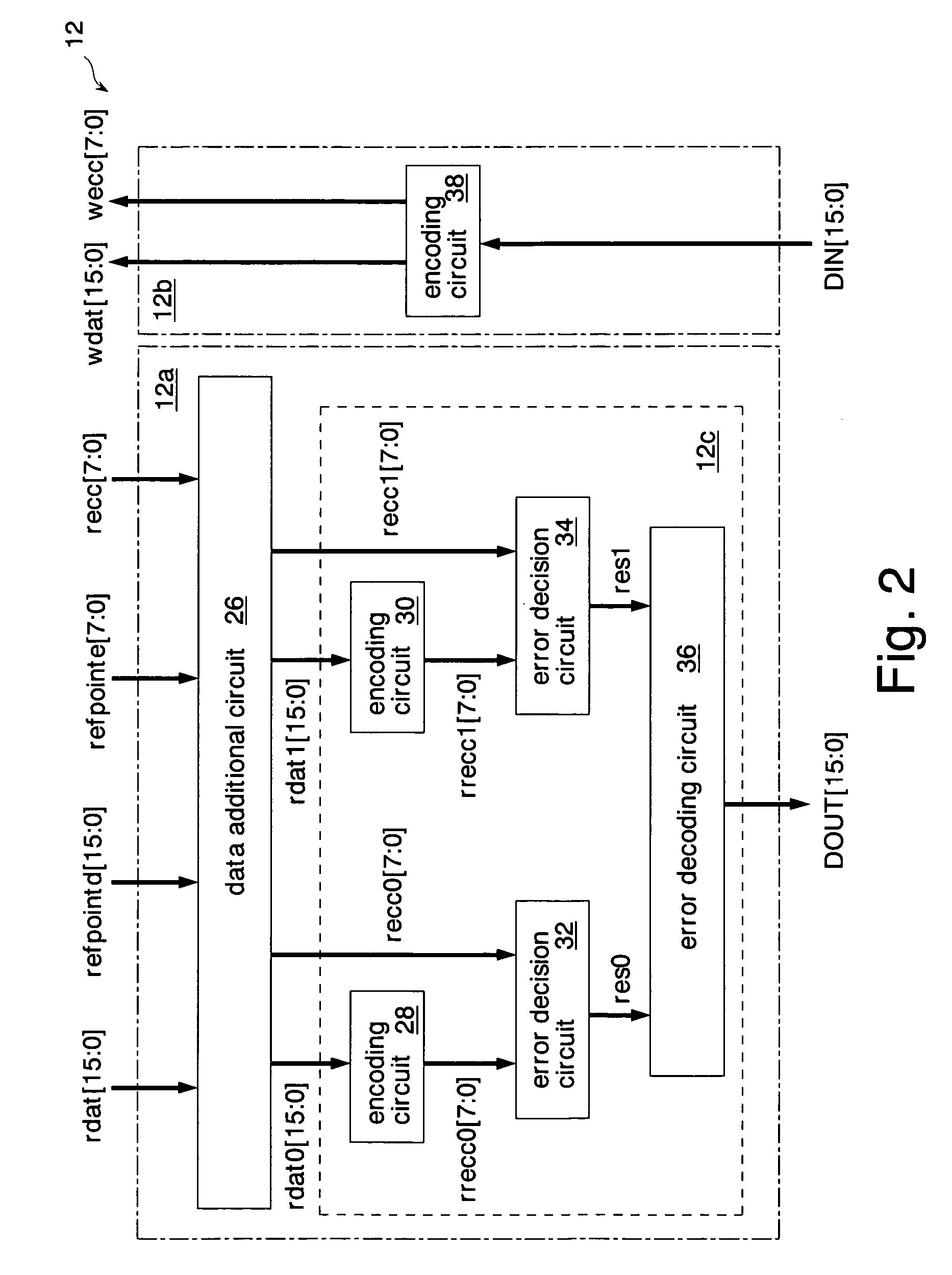
[0055]The pseudo SRAM has an address buffer 10, a data control circuit 12, a data input / output buffer 14, a command buffer 16, an access control circuit 18, a refresh control circuit 20, a clock buffer 22, and a memory core 24.

[0056]The memory core 24 has data blocks MBD0-15, code blocks MBE0-7, and a block control circuit BCNT. The data blocks MBD0-15 are formed corresponding to data terminals DQ15-0, respectively, and hold information data (hereinafter, also simply referred to as data) supplied through the data terminals DQ15-0, respectively. The code blocks MBE0-7 hold each bit of an error correction code in 8 bits generated by the data retained in the data blocks MBD0-15, respectively. The error correction code is used as code data for decoding information data stored in the d...

second embodiment

[0168]The memory core 24B is identical to the memory core 24A of the second embodiment, except that a row redundancy circuit that eliminates defects in a word line and a column redundancy circuit that eliminates defects in a bit line are formed.

[0169]The oscillator 40B self-oscillates a clock signal OSC having a shorter period than in the second embodiment. For this reason, an activation interval of each refresh point signal refpoint [21:0] output by the refresh control circuit 20A and a generation interval of the refresh request signal ref [21:0] are shorter than those in the second embodiment. Specifically, the activation interval T1 of each refresh point signal refpoint [21:0] (corresponding to the refresh interval of each memory cell) is set to be shorter than the data retention time of the worst memory cell. For this reason, all memory cells including the worst memory cell can always hold data by performing the refresh operation. The error correction function of the data contro...


PUM


Abstract

A data additional circuit adds plural types of expectation data to be read from a refresh block to data read from other blocks, respectively, to generate plural read data strings. An error correction circuit detects errors for each read data string, and sets the most reliable result of the error detection results to be true. The error correction circuit decodes data to be read from the refresh block based on a true error detection result. Moreover, the error correction circuit corrects the error of the read data string corresponding to the true error detection result. Consequently, without extending the read cycle time, a refresh operation can be hid, and errors can be corrected simultaneously. By correcting a data error read from a bad memory cell of data retention characteristics, a refresh request interval can be extended, and power consumption during a standby period can be reduced.

Description

CROSS REFERENCE TO RELATED APPLICATION[0001]This application is a continuation application of International Application No. PCT / JP03 / 10412, filed Aug. 18, 2003, and designating the U.S.BACKGROUND OF THE INVENTION[0002]1. Field of the Invention[0003]The present invention relates to a semiconductor memory having dynamic memory cells that require a refresh operation and a method for operating the same.[0004]2. Description of the Related Art[0005]Recently, a semiconductor memory referred to as a pseudo SRAM has been drawing attention. The pseudo SRAM has DRAM memory cells, operating as an SRAM that automatically executes an internal refresh operation of the memory cells. Because the dynamic memory cell has a small size, the bit cost is low, and accordingly, it is possible to develop the pseudo SRAM having a large capacity.[0006]However, since the pseudo SRAM stores data with charges accumulated in a capacitor of the memory cell, data might be lost due to charge leakage and so on. To avo...

Claims


Application Information

Patent Timeline
Patent Type & Authority Patents(United States)
IPC IPC(8): G11C7/00G11C7/10G11C11/406G11C11/4076G11C29/52
CPCG11C7/1006G11C11/406G11C11/40603G11C11/40615G11C11/40618G11C11/4076G11C29/52G11C2207/104G11C2211/4061G11C2211/4062G11C2211/4067
Inventor ETO, SATOSHI
Owner SOCIONEXT INC
Why Eureka
Try Eureka