Organic light-emitting diode and method of fabricating the same

a light-emitting diode and organic technology, applied in the manufacture of electric discharge tubes/lamps, discharge tubes luminescnet screens, electrode systems, etc., can solve the problems of reducing illumination efficiency, reducing inner light transmittance, and light consumption, so as to reduce total reflection and exterior glare, and improve element performance

Active Publication Date: 2007-04-17
XIAMEN TIANMA DISPLAY TECH CO LTD
View PDF8 Cites 11 Cited by
  • Summary
  • Abstract
  • Description
  • Claims
  • Application Information

AI Technical Summary

Benefits of technology

[0008]In order to solve the conventional problems, an object of the invention is to provide an OLED to reduce the total reflection and exterior glare, improving element performance thereof.
[0010]The protrusions formed on the substrate in the present invention are defined by photomask patterns, and may be arced, trapezoidal, or rectangular, and have proper sizes. Detailed characteristics of the protrusions are described in the subsequent embodiments. Referring to FIG. 2, the protrusions 20 formed on the substrate surface can decrease the incident angle θ1 and refractive angle θ2 to reduce the total reflection of inner light, improving light transmittance. Additionally, after exterior light reaches the uneven protrusion surfaces, it presents uniform scatter phenomenon to avoid exterior glare.
[0013]In the present invention, the protrusions facilitating light transmittance are directly fabricated on the substrate. Compared to the related art, requiring installation of an additional DBR, the invention provides a simpler and lower-cost process. In addition, the scatter effect of elements can be improved without extra fabrication process.

Problems solved by technology

For an organic light-emitting diode (OLED) featuring self-illumination, some inner light in a pixel cannot be emitted due to the total reflection phenomenon, resulting in light consumption and reduced illumination efficiency.
Currently, although a polarizer is used to reduce the exterior light effect, it may reduce the inner light transmittance, deteriorating illumination efficiency.
Nevertheless, DBR 15 may focus light at specific angles causing the exterior glare, deteriorating the quality of gray level or contrast, and further increasing the process cost.

Method used


Image

  • Organic light-emitting diode and method of fabricating the same
  • Organic light-emitting diode and method of fabricating the same
  • Organic light-emitting diode and method of fabricating the same

Examples


first embodiment

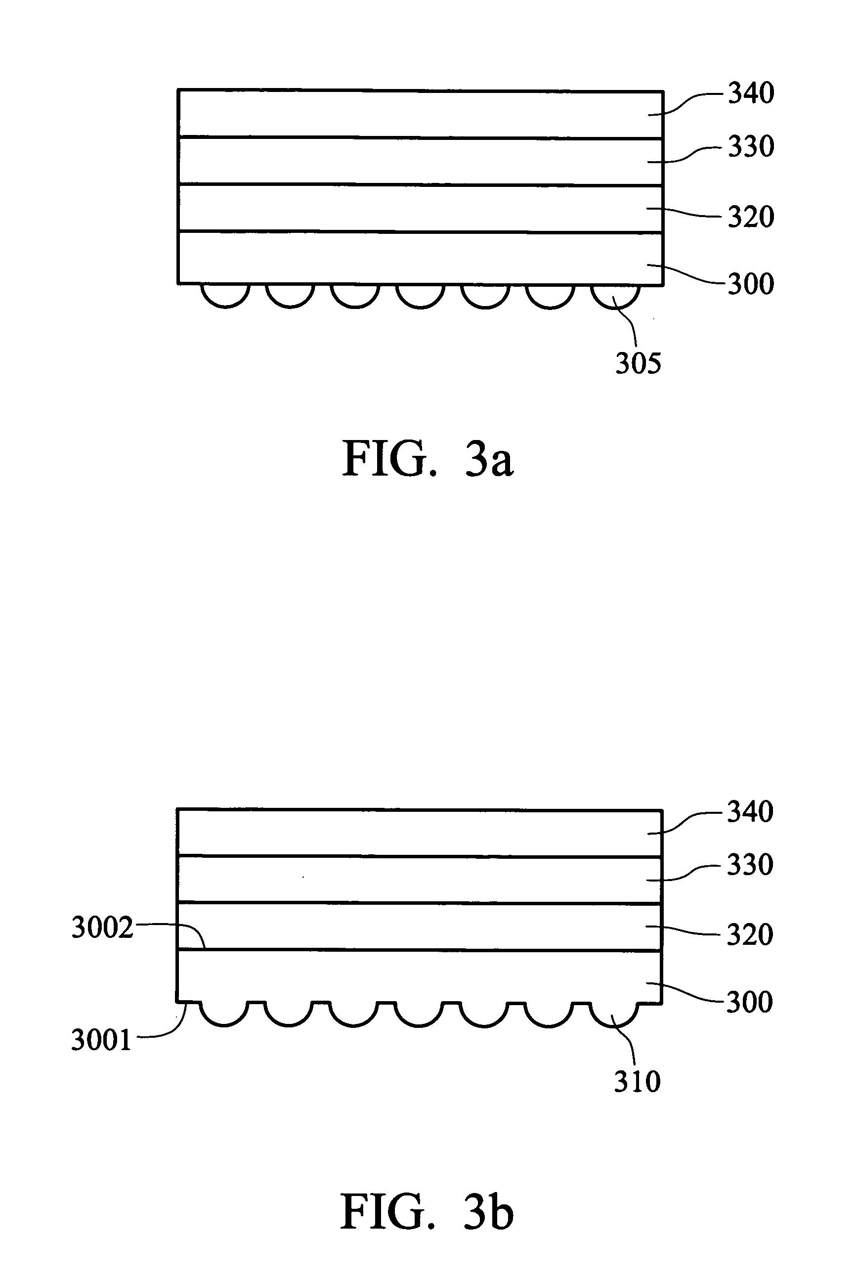
[0027]FIGS. 3a˜3b are cross sections of the method of fabricating the OLED according to the first embodiment of the invention. First, referring to FIG. 3a, a substrate 300 is provided. The substrate 300 includes a transparent glass substrate or plastic substrate, wherein the plastic substrate is composed of polyethyleneterephthalate, polyester, polycarbonates, polyimide, arton, polyacrylates, or polystyrene.

[0028]Next, a patterned resist layer 305 with, for example, an arced cross section, is formed on a first plane 3001 of the substrate 300, and other cross-sectional patterns are trapezoidal or rectangular, wherein arced cross section is preferable. Subsequently, the substrate 300 is defined to form a plurality of protrusions 310 on the first plane 3001 thereof with the patterned resist layer 305 used as an etching mask. The patterned resist layer 305 is then removed, as shown in FIG. 3b.

[0029]Detailed characteristics of protrusions, such as size, shape, or function are described ...

second embodiment

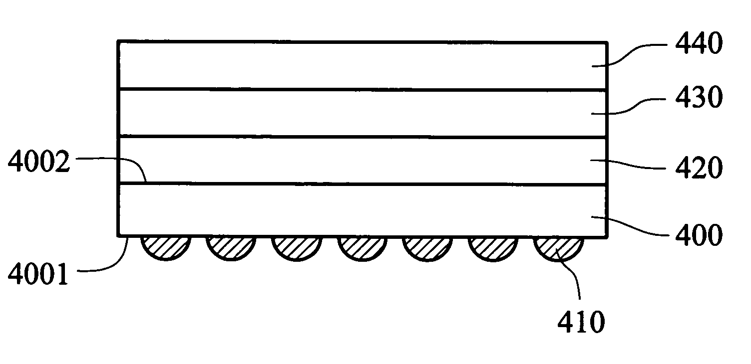
[0034]FIG. 4a is a cross sections of the method of fabricating the OLED according to the second embodiment of the invention. First, referring to FIG. 4a, a substrate 400 is provided. The substrate 400 includes a transparent glass substrate or plastic substrate, wherein the plastic substrate is composed of polyethyleneterephthalate, polyester, polycarbonates, polyimide, arton, polyacrylates, or polystyrene.

[0035]Next, a dielectric layer 410 is formed on a first plane 4001 of the substrate 400. The dielectric layer 410 is a transparent material, comprising silicon oxide, silicon nitride, or silicon oxide nitride. The refractive index of the dielectric layer 410 is altered with various substrate materials, about 1.3˜1.9, preferably 1.5. The thickness of the dielectric layer 410 is about 4000˜8000 Å, preferably 6000 Å. The dielectric layer 410 is formed by deposition, being a predetermined region of the subsequently formed protrusions.

[0036]Next, a patterned resist layer (not shown) is ...


PUM


Abstract

An organic light-emitting diode and method of fabricating the same. The organic light-emitting diode includes a substrate having a plurality of protrusions on a first plane thereof, a first electrode installed on a second plane of the substrate, wherein the second plane is opposed to the first plane, an organic light-emitting layer installed on the first electrode, and a second electrode installed on the organic light-emitting layer.

Description

BACKGROUND OF THE INVENTION[0001]1. Field of the Invention[0002]The present invention relates to an optoelectrical device, and more specifically to an organic light-emitting display and a method of fabricating the same.[0003]2. Description of the Related Art[0004]According to Snell's law n1*sin θ1=n2*sin θ2 (wherein n1 represents the refractive index of high-refractive materials, n2 represents the refractive index of low-refractive materials, θ1 represents the incident angle of light, θ2 represents the refractive angle of light), the total reflection of light may happen when light is transmitted from higher refractive index material to lower, for example, from glass or dielectric layer to the air. This is because the incident angle (θ1) of some light in the higher refractive index (n1) material is far enough over a critical angle so as to create light having a 90° refractive angle (θ2), wherein some incident light cannot enter the lower refractive index (n2) material.[0005]For an or...

Claims


Application Information

Patent Timeline
Patent Type & Authority Patents(United States)
IPC IPC(8): H05B33/00H01L51/52
CPCH01L51/5275H10K50/858
Inventor CHEN, JUI-HSING
Owner XIAMEN TIANMA DISPLAY TECH CO LTD
Why Eureka
Try Eureka