Liquid crystal display device having partition walls

a liquid crystal display and partition wall technology, applied in the direction of radio frequency controlled devices, optics, instruments, etc., can solve the problems of difficult to reduce the manufacturing cost in the conventional manufacturing method, poor utilization efficiency of raw materials, and increased processing costs, so as to facilitate the formation and reduce the manufacturing cost of the device

Inactive Publication Date: 2007-04-24
SEIKO EPSON CORP
View PDF24 Cites 21 Cited by
  • Summary
  • Abstract
  • Description
  • Claims
  • Application Information

AI Technical Summary

Benefits of technology

[0026]It is preferable that the aforementioned partition wall is a black-colored polyimide film formed by applying a thermosetting polyimide precursor mixed with a black coloring material therein to the substrate and performing a thermal treatment. In addition, it is preferable that the partition wall is a black-colored polyimide film formed by applying a photo-curing polyimide precursor mixed with a black coloring material therein to the substrate and performing light irradiation. In such a manner, it is possible that the partition wall having a light-shielding property can be easily formed.
[0027]In the partition wall formation process, it is preferable that an insulating film is formed on the substrate and openings are formed in the insulating film to expose regions for elements using the liquid material, thereby forming a partition wall. In such a manner, it is possible that the partition wall surrounding the peripheries of the regions of the plurality of elements using the liquid material can be easily formed.
[0028]It is preferable that the aforementioned liquid material is provided by means of a droplet ejection method. Therefore, it is possible to supply the liquid material rapidly under the control of drop position and drop quantity.
[0029]Further, a device of the present invention is manufactured according any one of the aforementioned methods. By doing so, it is possible to reduce the manufacturing cost for the device. More particularly, a device of the present invention has the constitution described below. In other words, the device of the present invention comprises a plurality of elements formed on a substrate, in which partition walls are provided to surround the peripheries of at least some regions of the plurality of elements and to cover the other regions, and the partition wall are formed with a member having a light-shielding property.

Problems solved by technology

However, in this conventional manufacturing method, there are disadvantages in that (1) since the process comprising the film formation and the etching is repeated many times, the manufacturing time is long, (2) since much of the formed thin film is removed, the utilization efficiency of raw material is not good, and (3) since waste such as the etching solution is excessively generated, the processing cost thereof is increased.
These disadvantages make it difficult to reduce the manufacturing cost in the conventional manufacturing method.
These disadvantages become more remarkable as the glass substrate to be a basic material becomes larger with increase in screen size of the liquid crystal display device.
In the case that the partition wall is formed and the pixel electrode or the color filter is formed using a liquid material, a film thickness of the pixel electrode or the color filter may be not uniform at the vicinity of a wall formed with the partition wall, that is, the vicinity of the periphery of the pixel region and a transmittance at the portions may be also not uniform.

Method used


Image

  • Liquid crystal display device having partition walls
  • Liquid crystal display device having partition walls
  • Liquid crystal display device having partition walls

Examples


Embodiment Construction

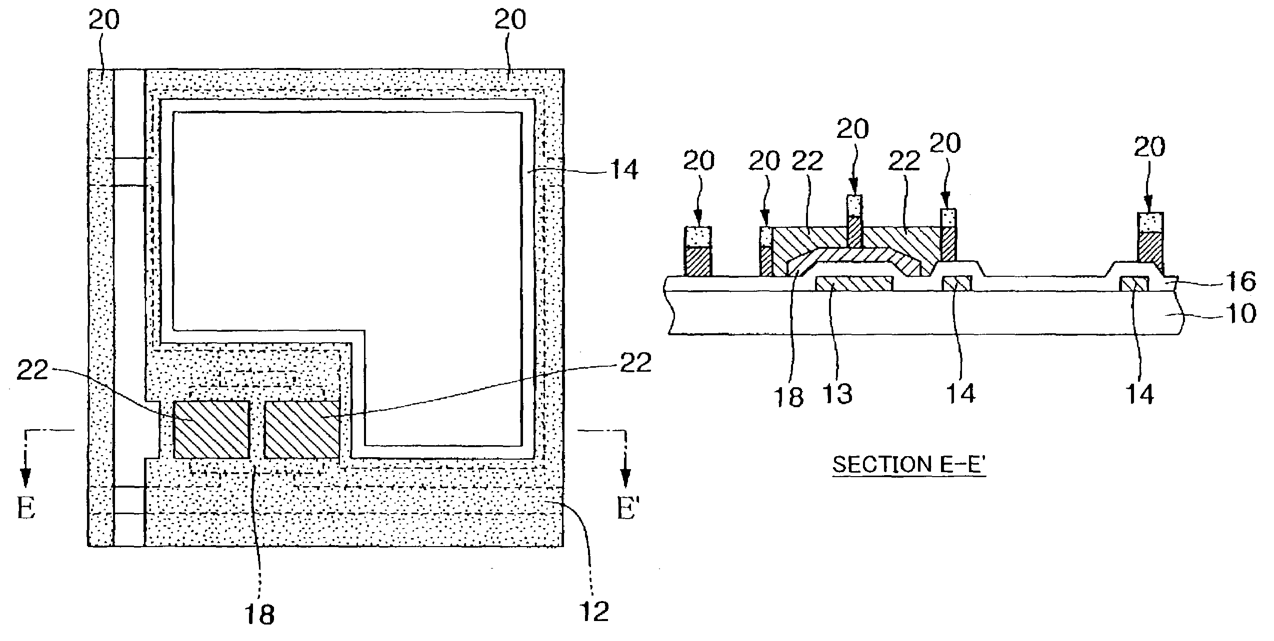
[0051]Now, a liquid crystal display device according to a first embodiment of the present invention and a method of manufacturing thereof will be described with reference to the accompanying drawings.

[0052]In the present invention, the droplet ejection method is a method of forming the desired pattern, including the ejected material, by ejecting droplets to a desired region and may be referred to as the inkjet method. In this case, the droplet to be ejected is not so-called ink used for printing, but a liquid material containing materials constituting the device, such materials include materials serving as, for example, the conductive material or insulating material constituting the device. Further, the droplet ejection is not limited to ejection by atomization, but includes continuous ejection of the liquid material drop by drop.

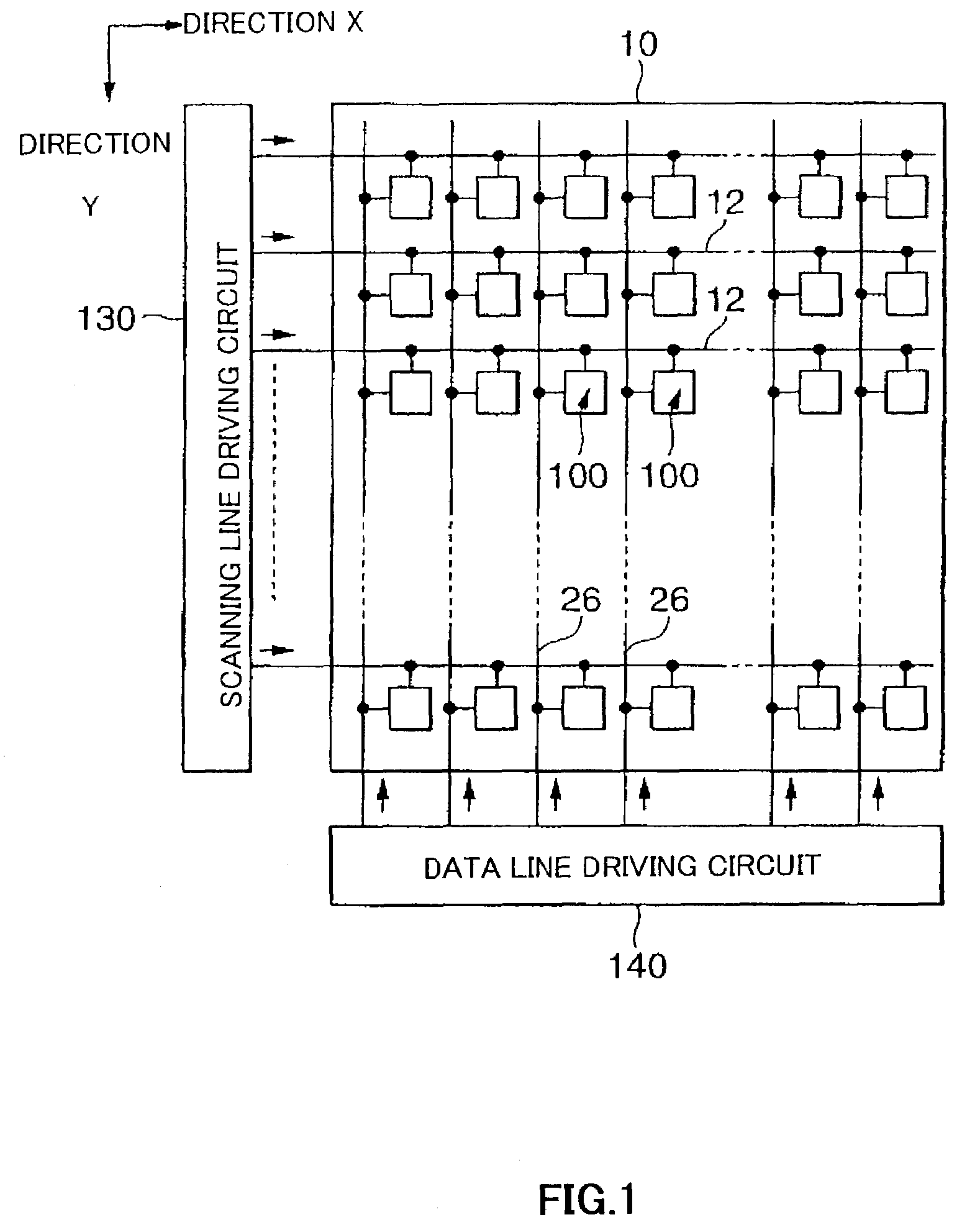
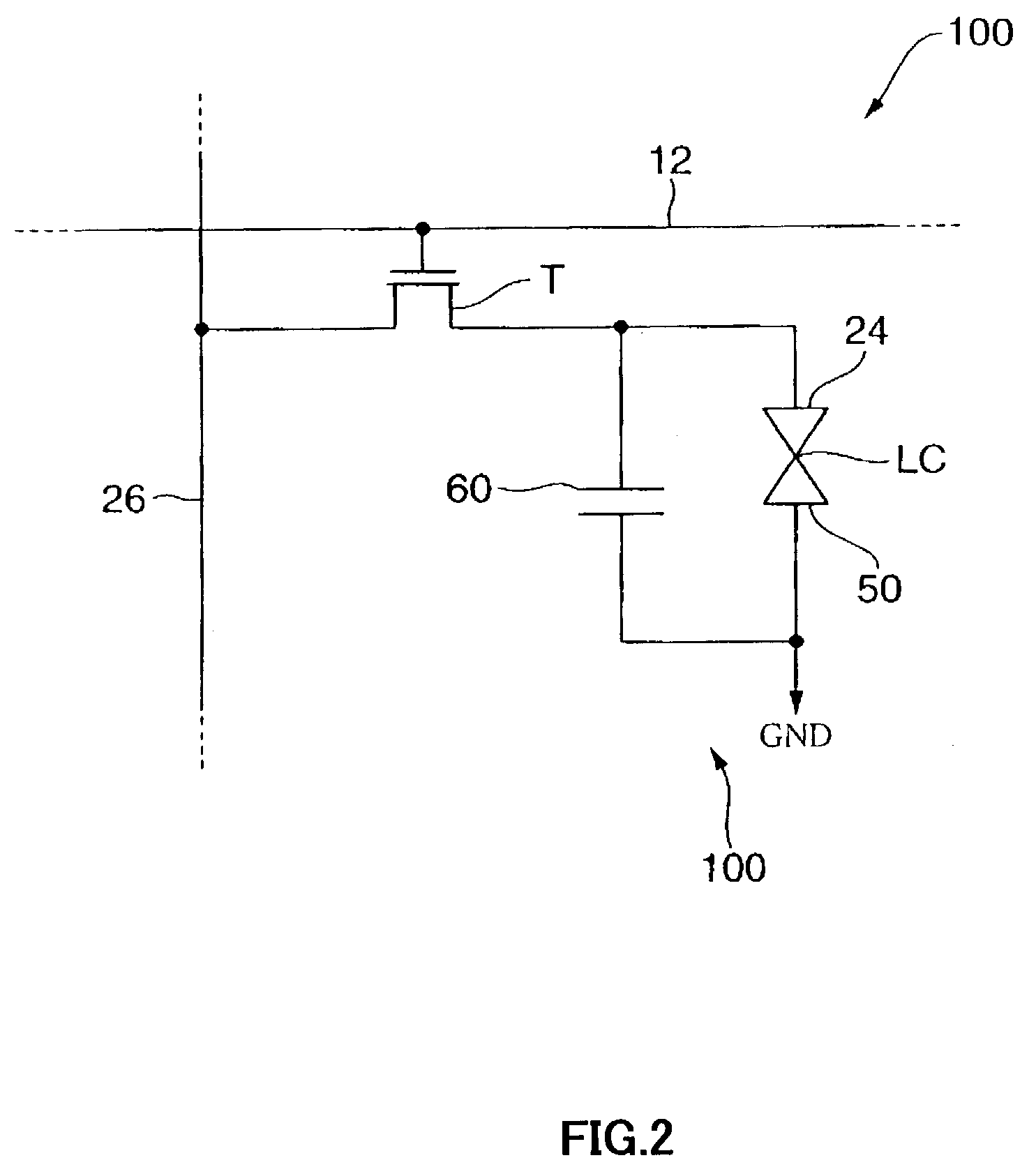
[0053]FIG. 1 schematically illustrates a configuration of a liquid crystal display device of this embodiment. The liquid crystal display device of this emb...


PUM

PropertyMeasurementUnit
diametersaaaaaaaaaa
thicknessaaaaaaaaaa
widthaaaaaaaaaa

Abstract

A liquid crystal display device 100 comprises a thin film transistor T, a source (data) line 26, a color filter 23, a pixel electrode 24 and the like. After a gate electrode 13, a gate insulating film 16, and a channel region 18 are formed on the glass substrate 10, a polyimide film 20 is formed to surround the peripheries of the region for forming the source/drain regions 22, the color filter 23, the pixel electrode 24, and the source line 26, respectively. A liquid material is applied to the regions surrounded with the wall made of the polyimide film 20 and a thermal treatment is performed to form the element of the color filter 23, the pixel electrode 24 and the like. The polyimide film 20 has a property of light-shielding and then has a function as a black matrix for shielding the surroundings of the pixel region.

Description

BACKGROUND OF THE INVENTION[0001]1. Technical Field of the Invention[0002]The present invention relates to a method of manufacturing a device (for example, a liquid crystal display device) comprising thin film elements such as thin film transistors, and to a device manufactured by means of the method.[0003]2. Description of the Related Art[0004]Liquid crystal display devices, which are electro-optical devices, have features of being thin and lightweight and have low power consumption, and thus they are used for various electronic apparatuses, such as personal computers, mobile phones, digital still cameras, and liquid crystal televisions.[0005]The liquid crystal display device is provided with pixel portions using active elements such as thin film transistors. As the thin film transistor constituting the pixel portion, the inversely staggered type (or bottom gate type) structure constructed by forming a gate electrode on a substrate and laminating a semiconductor layer such as a cha...

Claims


Application Information

Patent Timeline
Patent Type & Authority Patents(United States)
IPC IPC(8): H01L29/04H01L31/036H01L31/0376H01L31/112G02F1/1335G02F1/1362G02F1/1368H01L21/77H01L21/84H01L27/12H01L27/144H01L27/146H01L29/786H01L31/0216
CPCG02F1/136209H01L27/12H01L27/1446H01L27/1248H01L27/14683H01L29/78633H01L31/02164H01L27/14621G02F2001/136222G02F1/136222
Inventor FURUSAWA, MASAHIRO
Owner SEIKO EPSON CORP
Why Eureka
Try Eureka