Image-sensor signal processing circuit

a signal processing circuit and image sensor technology, applied in the direction of instruments, pulse techniques, radio control devices, etc., can solve the problems of increasing the size, increasing the cost of the camera system, etc., and achieve the effect of flexible coping

Active Publication Date: 2007-04-24
HITACHI DISPLAYS +1
View PDF10 Cites 56 Cited by
  • Summary
  • Abstract
  • Description
  • Claims
  • Application Information

AI Technical Summary

Benefits of technology

[0014]An object of the present invention is to provide a semiconductor integrated circuit device capable of flexibly coping with the signal processing of both image sensors of the CCD sensor and the CMOS sensor without using any external circuits.

Problems solved by technology

Therefore, an additional external component is required to cope with the sensor output of the CMOS sensor in the signal-processing circuit for the CCD sensor, and so there arises the problem of cost increase and size increase, etc. of the camera system.

Method used


Image

  • Image-sensor signal processing circuit
  • Image-sensor signal processing circuit
  • Image-sensor signal processing circuit

Examples


first embodiment

[0052](First Embodiment)

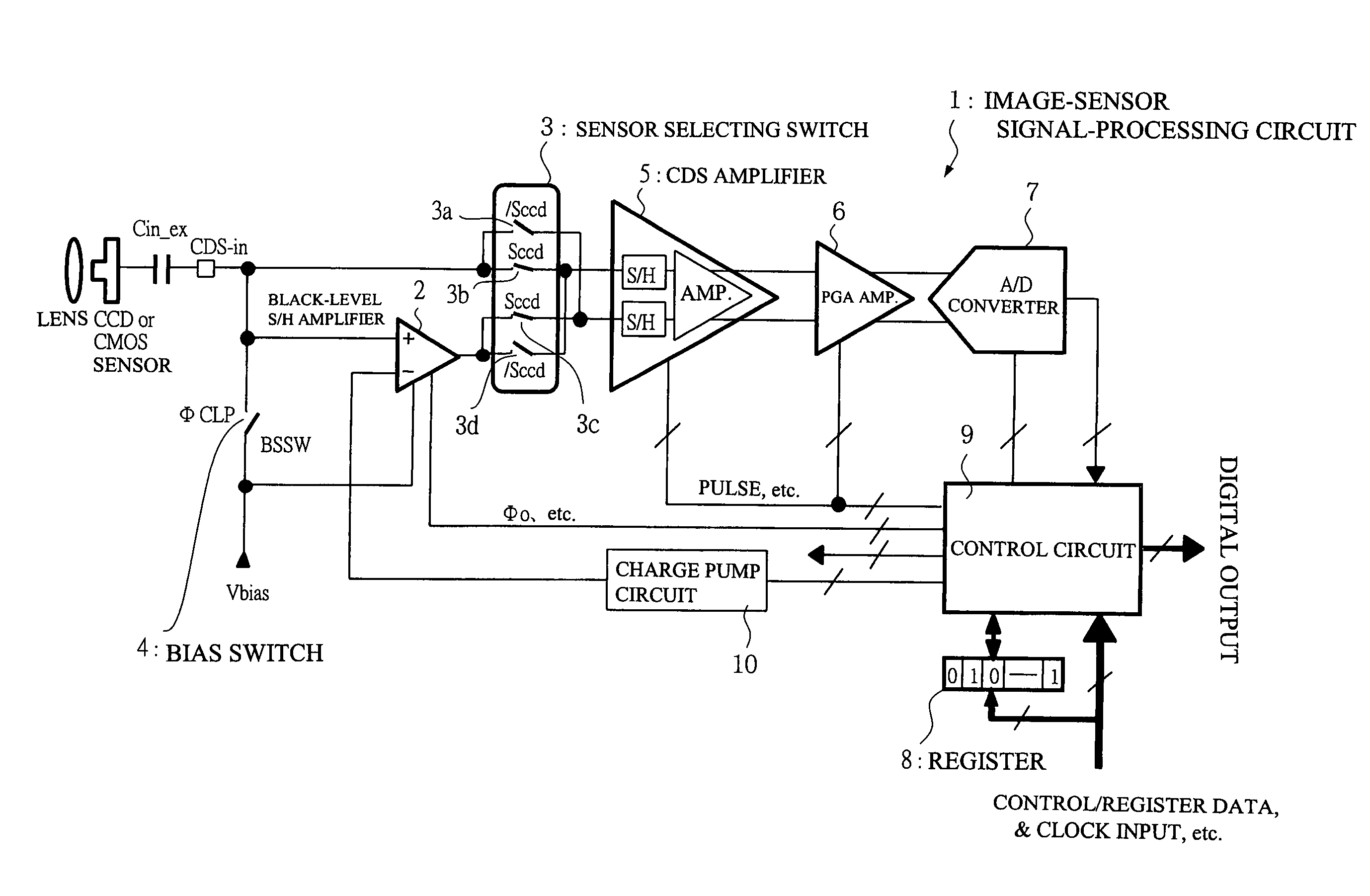
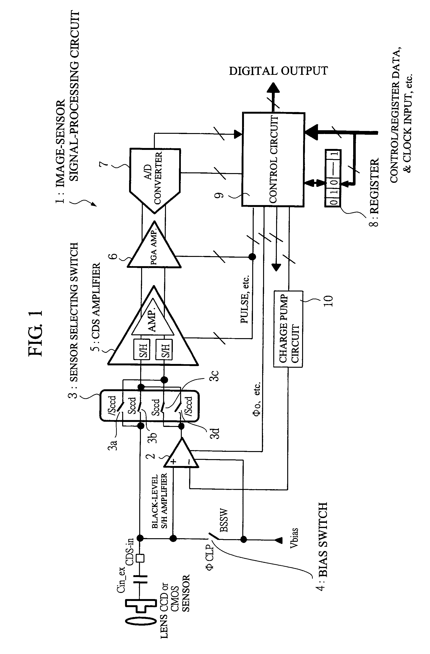
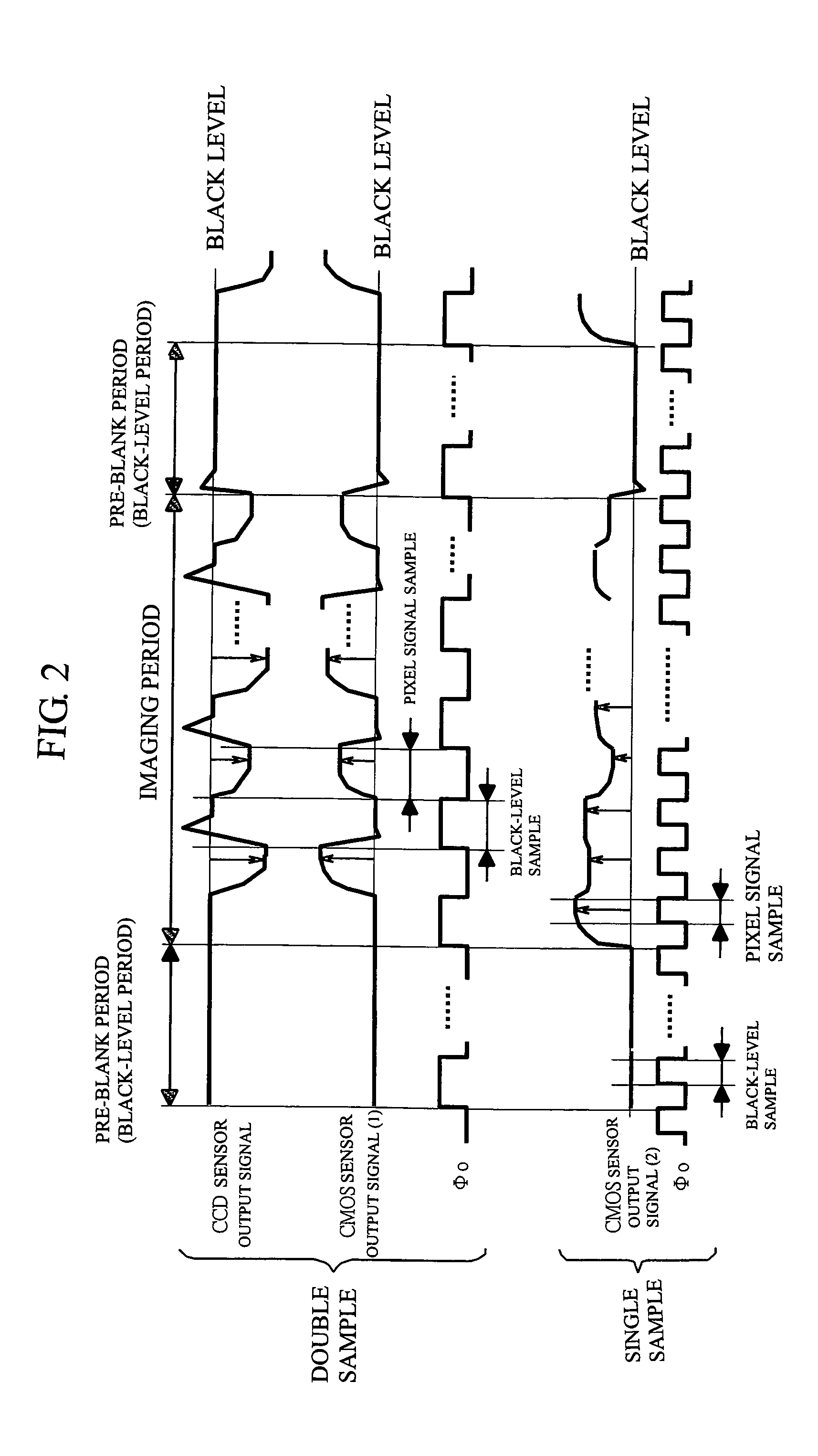
[0053]FIG. 1 is a block diagram showing an image-sensor signal-processing circuit according to a first embodiment of the present invention; FIG. 2 is an explanatory diagram of signal-output waveforms of a CCD sensor and a CMOS sensor in the image-sensor signal-processing circuit in FIG. 1; FIG. 3 is a timing chart at the time of selecting the CCD sensor in the image-sensor signal-processing circuit in FIG. 1; FIG. 4 is a block diagram showing another configuration example of the image-sensor signal-processing circuit in FIG. 1; and FIG. 5 is a timing chart at the time of selecting the CCD sensor in the image-sensor signal-processing circuit in FIG. 4.

[0054]In this first embodiment, an image-sensor signal-processing circuit 1 provided in a semiconductor integrated circuit device comprises, as shown in FIG. 1, a black-level sample / hold (S / H) amplifier 2, a sensor selecting switch (sensor selecting section) 3, a bias switch (first bias switch) 4, a CDS amplifier...

second embodiment

[0099](Second Embodiment)

[0100]FIG. 6 is a block diagram showing an image-sensor signal-processing circuit according to a second embodiment of the present invention and FIG. 7 is a timing chart at the time of selecting the CCD sensor in the image-sensor signal-processing circuit in FIG. 6.

[0101]According to a second embodiment, the image-sensor signal-processing circuit 1b is, as shown in FIG. 6, one in which a bias voltage almost equal to the bias voltage Vbias is applied to the terminal CDS-in by the bias amplifier 11 when the output signal of the image sensor is inputted via the capacitor Cin_ex.

[0102]An image-sensor signal-processing circuit 1b is obtained by newly adding a bias amplifier 11 and a bias switch (second bias switch) 12 to the configuration comprising the black-level S / H amplifier 2, the sensor selecting switch 3, the bias switch 4, the CDS amplifier 5, the PGA amplifier 6, the A / D converter 7, the register 8, the control circuit 9, and the charge pump circuit 10 si...

third embodiment

[0112](Third Embodiment)

[0113]FIG. 8 is a block diagram showing an image-sensor signal-processing circuit according to a third embodiment of the present invention, and FIG. 9 is a timing chart at the time of selecting the CCD sensor in the image-sensor signal-processing circuit in FIG. 8.

[0114]In a third embodiment, an image-sensor signal-processing circuit 1c can select the output voltage of the black-level S / H amplifier 2 depending on the image sensor (CCD sensor or CMOS sensor) in the case of the biasing by the use of the bias amplifier 11 shown in FIG. 6.

[0115]The image-sensor signal-processing circuit 1c is obtained by newly adding bias switches 14 to 17 to the configuration comprising the black-level S / H amplifier 2, the sensor selecting switch 3, the CDS amplifier 5, the PGA amplifier 6, the A / D converter 7, the register 8, the control circuit 9, the charge pump circuit 10, the bias amplifier 11, and the bias switch 12 as shown in the image-sensor signal-processing circuit 1b...


PUM


Abstract

By flexibly coping with both image sensors of a CCD sensor and a CMOS sensor without providing any external circuit, a signal processing is performed. In a sensor selecting switch provided in an image-sensor signal-processing circuit, first and fourth switches are turned on when the CMOS sensor is connected, and second and third switches are turned on when the CCD sensor is connected. The sensor selecting switch is controlled by a control signal generated in a control circuit, based on sensor selection data which is stored in a register and which is data for selecting the CCD or CMOS sensor. By so doing, even if polarity of an output signal of the image sensor is reversed, a normal signal is inputted to both inputs of the CDS amplifier, whereby it is possible to flexibly cope with both of the CCD and CMOS sensors.

Description

CROSS-REFERENCE TO RELATED APPLICATION[0001]The present application claims priority from Japanese Patent Application No. JP 2003-153412 filed on May 29, 2003, the content of which is hereby incorporated by reference into this application.BACKGROUND OF THE INVENTION[0002]The present invention relates to a semiconductor integrated circuit device and a digital camera system and, particularly, to a technique effectively applied to an analog front-end signal processing of a CCD sensor and a CMOS sensor.[0003]The CCD (Charge Coupled Device) sensor is widely used as an electronic imaging device in such a camera system as a video camera, a digital still camera, and a camera-equipped cell phone.[0004]In an image-sensor signal-processing circuit provided in the digital video camera, for example, it is well known that signals taken from an imaging device such as a CCD sensor are sampled with respect to color levels by a correlated double sampling circuit etc.[0005]This correlated double sampli...

Claims


Application Information

Patent Timeline
Patent Type & Authority Patents(United States)
IPC IPC(8): G11C27/02H04N5/335H04N5/369H01L27/146H04N5/372H04N5/374H04N5/378H04N101/00
CPCH04N5/335H04N25/00
Inventor IMAIZUMI, EIKIANBO, TAKANOBUSONE, YASUHIKOMATSUURA, TATSUJIODAKA, TERUAKI
Owner HITACHI DISPLAYS
Why Eureka
Try Eureka