Method of fabricating ohmic contact on n-type gallium nitride (GaN) of room temperature by plasma surface treatment

a technology of gan and gallium nitride, which is applied in the field of plasma surface treatment of gan of room temperature, can solve the problem of only being able to obtain such low contact resistivity, and achieve the effect of reducing potential barrier, low contact resistivity, and low contact resistan

Inactive Publication Date: 2007-05-08
SUZHOU LEKIN SEMICON CO LTD
View PDF9 Cites 20 Cited by
  • Summary
  • Abstract
  • Description
  • Claims
  • Application Information

AI Technical Summary

Benefits of technology

[0008]The present invention as illustrated in FIG. 2 comprises a new method of fabricating ohmic contacts by treating the n-type GaN surface using an Inductively Coupled Plasma (ICP) process before ohmic metal formation on the n-type GaN surface. By utilizing this new technique in the n-type ohmic contact formation on the GaN, very low contact resistivity of 9.4×10⁻⁶ ohmcm2 was obtained using ICP treatment with chlorine gas, prior to the deposition of Ti and Al metals. Obtaining such low contact resistivity is only possible with a high temperature heat treatment process used in conventional techniques. After the ICP treatment, it has been observed that nitrogen vacancies, which formed during ICP treatment, play an important role in reducing potential barrier and increasing the number of electrons in the metal and semiconductor interface, hence enabling electron conduction by tunneling effect leads to form an ohmic contact.

Problems solved by technology

Obtaining such low contact resistivity is only possible with a high temperature heat treatment process used in conventional techniques.

Method used


Image

  • Method of fabricating ohmic contact on n-type gallium nitride (GaN) of room temperature by plasma surface treatment
  • Method of fabricating ohmic contact on n-type gallium nitride (GaN) of room temperature by plasma surface treatment
  • Method of fabricating ohmic contact on n-type gallium nitride (GaN) of room temperature by plasma surface treatment

Examples


Embodiment Construction

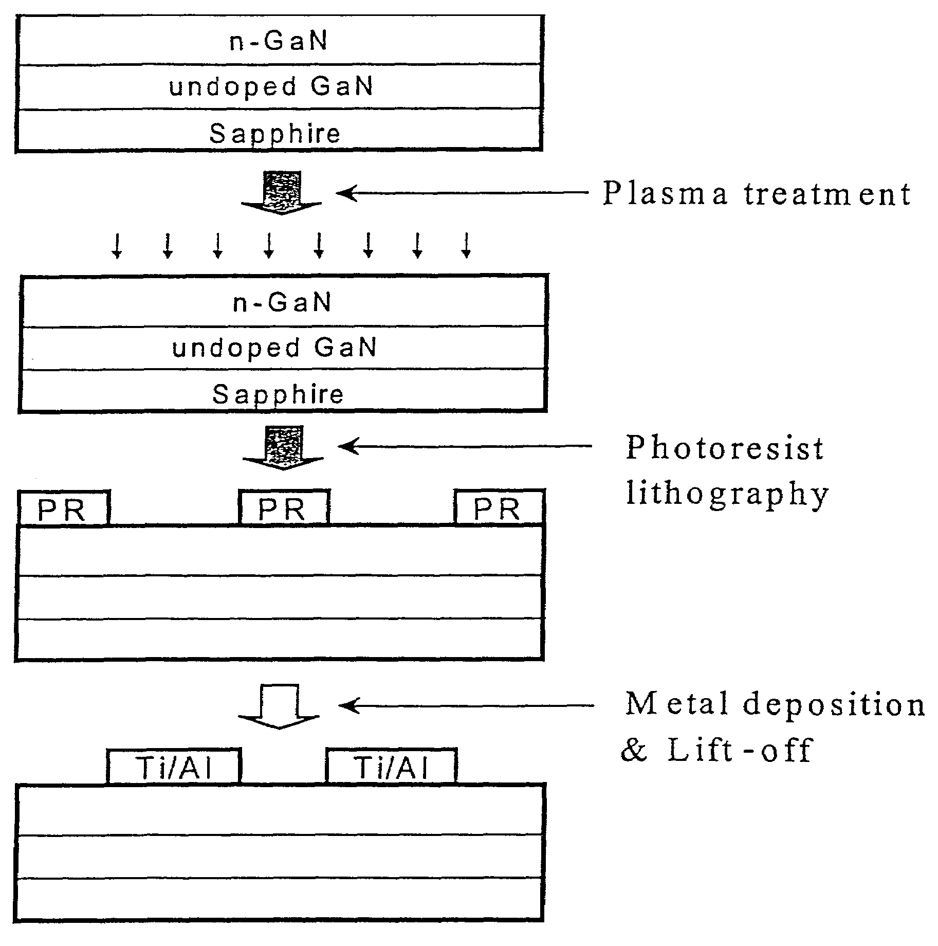
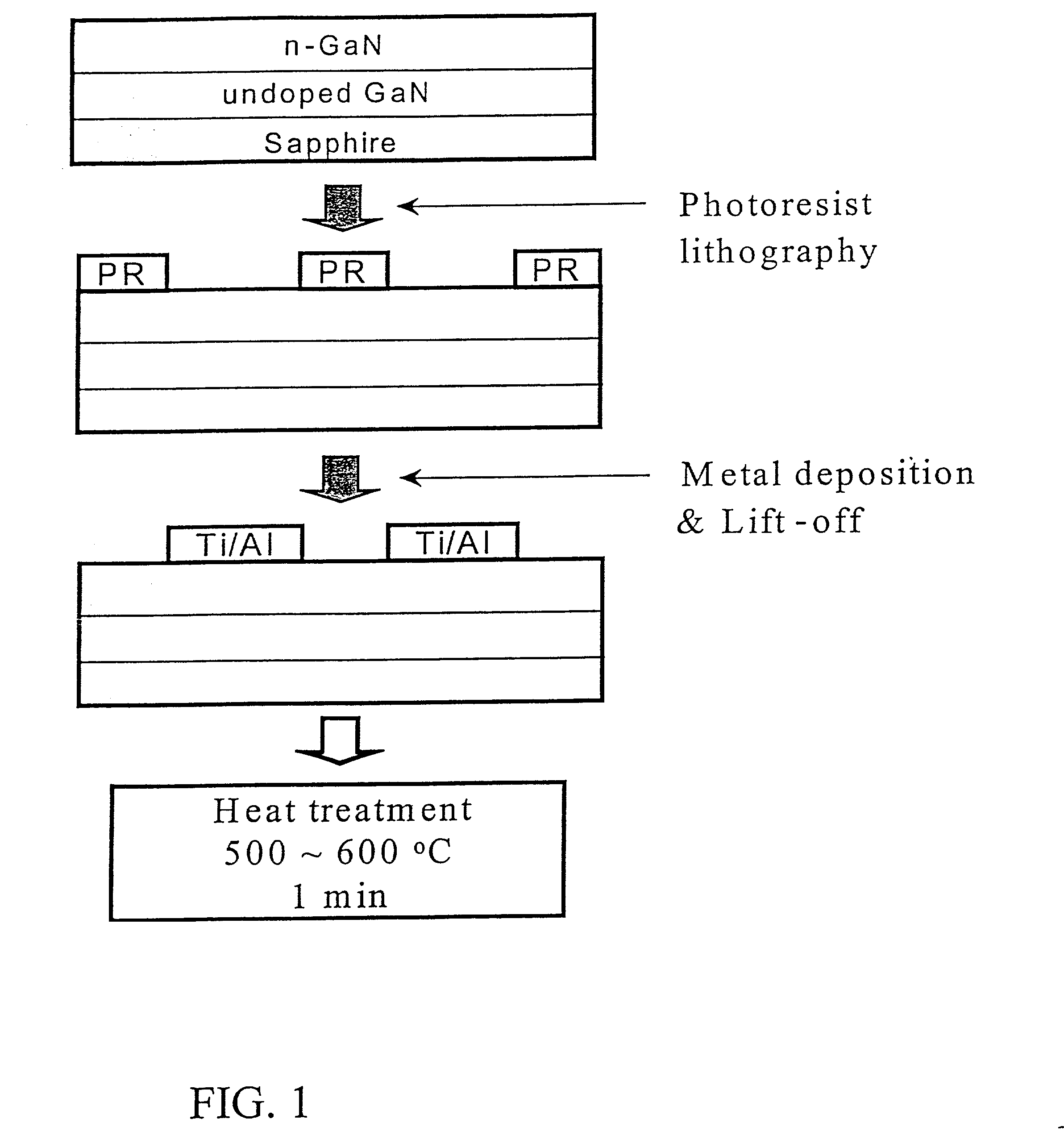
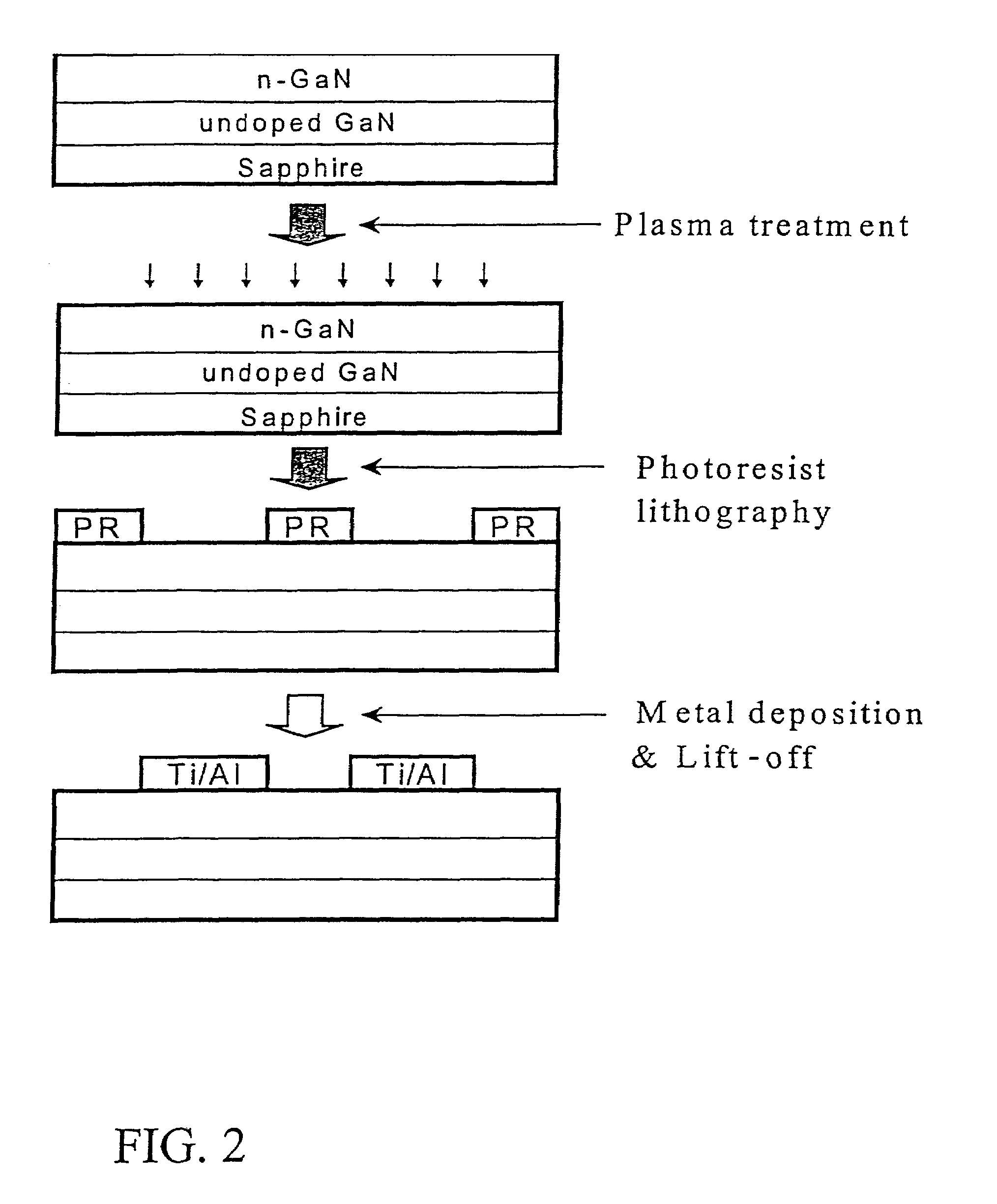
[0022]Reference will now be made in detail to an embodiment of the present invention, example of which is illustrated in the accompanying drawings.

[0023]As shown in FIG. 2, room-temperature Ti / Al ohmic contact on n-type GaN was obtained by the surface treatment using Cl2 inductively-coupled plasma treatment. The specific contact resistivity was dramatically decreased from Schottky behavior to 9.4×10⁻⁶ Ωcm2 by the treatment. The binding energy of Ga—N bond and the atomic ratio of Ga / N were simultaneously increased after the plasma treatment. This provides evidence that N vacancies, acting as donor for electrons, were produced at the etched surface, resulting in shift of Fermi level to the near from conduction band. This leads to the reduction in contact resistivity through the decrease of Schottky barrier for the conduction of electrons.

[0024]Obtaining ohmic contacts on GaN based devices exhibiting low contact resistivity has attracted substantial interest due to the potential of imp...


PUM

PropertyMeasurementUnit
pressureaaaaaaaaaa
thicknessaaaaaaaaaa
carrier concentrationaaaaaaaaaa

Abstract

Forming low contract resistance metal contacts on GaN films by treating a GaN surface using a chlorine gas Inductively Coupled Plasma (ICP) etch process before the metal contacts are formed. Beneficially, the GaN is n-type and doped with Si, while the metal contacts include alternating layers of Ti and Al. Additionally, the GaN film is dipped in a solution of HCl:H2O prior to metal contact formation.

Description

[0001]This application claims the benefit of U.S. Provisional Patent Application No. 60 / 278,468 filed on Mar. 23, 2001, which is hereby incorporated by reference for all purposes as if fully set forth herein.BACKGROUND OF THE INVENTION[0002]1. Field of the Invention[0003]The present invention relates to a method of fabricating ohmic contact on n-type gallium nitride (GaN) of room temperature by plasma surface treatment.[0004]2. Discussion of the Related Art[0005]Metal contact is one of the most important processes in fabricating opto-electronic devices and high-temperature, high power electronic devices using gallium nitride (GaN)—based compound semiconductors. In particular, ohmic metal contacts with low specific contact resistivity are essential to obtain high performance devices. The ohmic contact is strongly dependent on the interfacial property between metal contacts and the semiconductors. Despite numerous attempts to improve metal contact property, it has been very difficult ...

Claims


Application Information

Patent Timeline
Patent Type & Authority Patents(United States)
IPC IPC(8): H01L21/44H01L21/285
CPCH01L21/28575
Inventor LEE, JONG LAMJANG, HO WONKIM, JONG KYUJEON, CHANGMIN
Owner SUZHOU LEKIN SEMICON CO LTD
Why Eureka
Try Eureka