Ferroelectric thin film element, piezoelectric actuator and liquid discharge head

a technology of ferroelectric thin film and actuator, which is applied in the direction of piezoelectric/electrostrictive device details, device material selection, device details, etc., can solve the problems of increasing the spontaneous polarization unable to improve the residual polarization or fatigue resistance and unable to obtain satisfactory device characteristics of the ferroelectric thin film. , to achieve the effect of improving the characteristics of the ferroelectric thin

Inactive Publication Date: 2007-05-08
CANON KK
View PDF20 Cites 14 Cited by
  • Summary
  • Abstract
  • Description
  • Claims
  • Application Information

AI Technical Summary

Benefits of technology

[0017]An object of the present invention is to provide a ferroelectric thin film element which not subject to deterioration of its characteristics upon application of a small stress applied in the ferroelectric thin film along a planar direction of the substrate, shows a high spontaneous polarization of the ferroelectric thin film and is suitable for thin film formation. It is effective for an element in which the spontaneous polarization of the ferroelectric thin film is involved in improving the characteristics of the ferroelectric thin film element, for example, a non-volatile memory. In heteroepitaxial growing technology, it is preferable to reduce the stress generated in the vicinity of the boundary between the substrate and the formed ferroelectric thin film and applied along the planar direction of the substrate. It is estimated that the stress generated by a misfit in the crystal lattices between the substrate and the ferroelectric thin film and applied in the planar direction of the substrate constitutes a cause of film peeling of the ferroelectric thin film, so that such film peeling can be prevented by a reduction in the aforementioned stress applied in the planar direction of the substrate.
[0018]Another object of the present invention is to provide a ferroelectric thin film element having a substrate and an epitaxial ferroelectric thin film provided on the substrate, in which the epitaxial ferroelectric thin film (1) satisfies a relation z/z0>1.003, wherein a crystal face parallel to a crystal face of a surface of the substrate, among crystal faces of the epitaxial ferroelectric thin film, is taken as a Z crystal face, a face spacing of the Z crystal face is taken as z and a face spacing of the Z crystal face of a material constituting the epitaxial ferroelectric thin film in a bulk state is taken as z0, and (2) also satisfies a relation 0.997≦x/x0≦1.003, wherein one of the crystal faces of the epitaxial ferroelectric thin film perpendicular to the Z crystal face is taken as an X crystal face, a face spacing of the X crystal face is taken as x and a face spacing of the X crystal face of the material constituting the epitaxial ferroelectric thin film in a bulk state is taken as x0. (It is understood that the term “crystal face” used herein is interchangeable with the term “crystal plane.”) According to the present invention, there can be obtained a ferroelectric thin film element free from deterioration of its characteristics, showing a high spontaneous polarization and suitable for thin film formation.
[0019]Still another object of the present invention is to provide a piezoelectric actuator having excellent characteristics, by forming an epitaxial ferroelectr

Problems solved by technology

However, even with an excellent ferroelectric thin film such as a PZT thin film, it is difficult to obtain satisfactory device characteristics in a ferroelectric thin film formed by a polycrystalline member, because of a distortion of physical properties at the crystal grain boundary.
These methods can cause a compression stress to be applied to the ferroelectric thin film, thereby increasing the spontaneous polarization of the ferroelectric thin film.
However the prior method of increasing the spontaneous polarization by applying a compression stress to the ferroelectric thin film, though capable of increasing the spontaneous polarization, cannot improve the deterioration in the residual polarization or the fatigue resistance of the ferroelectric thin film.
It is estimated that a stress applied in the ferroelectric thin film along a planar direction of the substrate is significantly involved in the aforementioned deterioration of the characteristics of the ferroelectric thin film, and, in case a large compression stress is applied to the ferroelectric thin film in the prior method, the stress applied along the planar direction of the substrate acts on the fer

Method used


Image

  • Ferroelectric thin film element, piezoelectric actuator and liquid discharge head
  • Ferroelectric thin film element, piezoelectric actuator and liquid discharge head
  • Ferroelectric thin film element, piezoelectric actuator and liquid discharge head

Examples


example 1

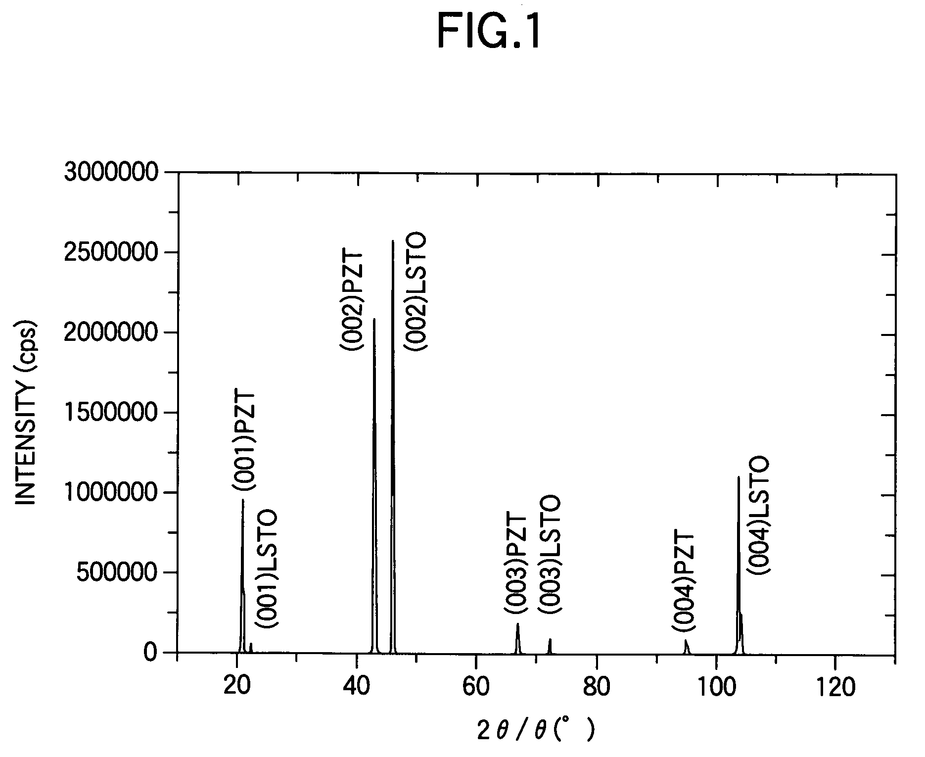
[0083]On a substrate (single crystal growing substrate) (La0.038, Sr0.962)TiO3 (100) serving also as an electrode, a PZT thin film of a thickness of 70 nm was epitaxially grown as an epitaxial ferroelectric thin film by a sputtering apparatus using an RF magnetron method, thereby obtaining a ferroelectric thin film element. In this operation, there were employed a substrate temperature of 600° C., an argon / oxygen ratio of 30 / 1 at film formation, a gas pressure of 0.2 Pa, an RF power of 0.8 W / cm2 at film formation and a cooling speed after film formation of 100° C. / min until 180° C. or lower was reached, and a pre-sputtering prior to film formation was conducted for 3 minutes with an RF power of 0.3 W / cm2. The PZT thin film, constituting the epitaxial ferroelectric thin film, had a composition of Pb(Zr0.52, Ti0.48)O3. The single crystal property of the PZT thin film of the thus prepared ferroelectric thin film element was measured by XRD. The obtained result is shown in FIG. 1. Based...

example 2

[0087]On a substrate (single crystal growing substrate) (La0.038, Sr0.962)TiO3 (100) serving also as an electrode, a PZT thin film of a thickness of 70 nm was epitaxially grown as an epitaxial ferroelectric thin film by a sputtering apparatus using an RF magnetron method, thereby obtaining a ferroelectric thin film element. In this operation, there were employed a substrate temperature of 600° C., an argon / oxygen ratio of 30 / 1 at film formation, a gas pressure of 0.2 Pa, an RF power of 0.8 W / cm2 at film formation and a cooling speed after film formation of 80° C. / min until 180° C. or lower was reached, and a pre-sputtering prior to film formation was conducted for 30 minutes with an RF power of 0.3 W / cm2. The PZT thin film, constituting the epitaxial ferroelectric thin film, had a composition of Pb(Zr0.52, Ti0.48)O3. The single crystal property of the PZT thin film of the thus prepared ferroelectric thin film element was measured by XRD. The obtained result is shown in FIG. 1. Based...

example 3

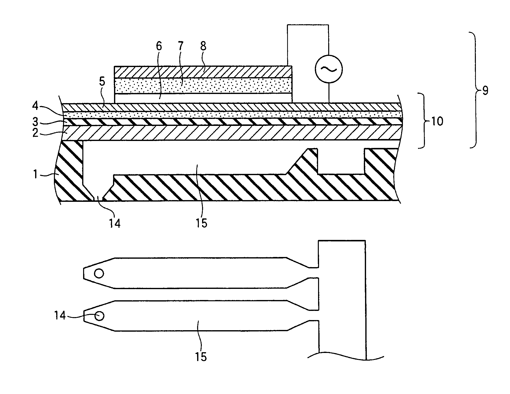
[0091]A mirror polished Si (100) of 15 mm square was employed as a substrate, and its surface was at first etched with tetramethylammonium hydroxide (also represented as TMAH) (manufactured by Kanto Chemical Co.) for 10 minutes at room temperature, then washed with purified water and rinsed with an acetone vapor bath. Then, on this substrate, a YZT thin film of a thickness of 10 nm was formed by a sputtering apparatus using an RF magnetron method at a substrate temperature of 800° C. An XRD measurement after film formation confirmed that the YSZ film had a crystal orientation rate of 99% or higher in a [100] direction. Then a Pt film of 100 nm as a lower electrode was formed by sputtering at a substrate temperature of 600° C. An XRD measurement after film formation confirmed that the Pt had a crystal orientation rate of 97% or higher in a [111] direction. Then, on these laminated films, a buffer layer of [PbTiO3] (also represented as PT) of 7 nm was formed with a sputtering apparatu...


PUM


Abstract

A ferroelectric thin film element comprises a substrate and an epitaxial ferroelectric thin film provided on the substrate. The thin film satisfies z/z0>1.003 and 0.997≦x/x0≦1.003, where a crystal face of said thin film parallel to a crystal face of a surface of the substrate is taken as a Z crystal face, a face spacing of the Z crystal face is taken as z, a face spacing of the Z crystal face of a material constituting the thin film in a bulk state is taken as z0, a crystal face of the thin film perpendicular to the Z crystal face is taken as an X crystal face, a face spacing of the X crystal face is taken as x and a face spacing of the X crystal face of the material constituting the thin film in a bulk state is taken as x0.

Description

BACKGROUND OF THE INVENTION[0001]1. Field of the Invention[0002]The present invention relates to a ferroelectric thin film element, and more particularly to an element in which a spontaneous polarization of a ferroelectric thin film is involved in an improvement in device characteristics, such as a non-volatile memory. The present invention also relates to a piezoelectric actuator utilizing a piezoelectric property of an epitaxial film and a liquid discharge head equipped with a piezoelectric actuator unit of a configuration including such a piezoelectric actuator.[0003]2. Description of the Related Art[0004]As a memory medium for a non-volatile memory and the like, there is recently desired a memory apparatus employing a ferroelectric thin film having a high performance (hereinafter called ferroelectric memory). For securing optimal device characteristics and reproducibility in the ferroelectric memory, the ferroelectric thin film is required to have a large spontaneous polarizatio...

Claims


Application Information

Patent Timeline
IPC IPC(8): H01L41/04H01L41/16H01L41/24H01L41/09H01L41/22H02N2/00
CPCH01L41/316H01L41/094H10N30/2042H10N30/076
Inventor IFUKU, TOSHIHIROFUKUI, TETSUROMATSUDA, TAKANORI
Owner CANON KK
Why Eureka
Try Eureka