
Method for fabricating a semiconductor product with a memory area and a logic area

a semiconductor and logic technology, applied in the field of semiconductor technology, can solve the problems of not being able to meet the specific requirements of fe transistors provided for logic and memory applications, particularly stringent fabrication process requirements, etc., and achieve the effect of high uniform doping

Inactive Publication Date: 2007-05-15
POLARIS INNOVATIONS
View PDF17 Cites 12 Cited by
  • Summary
  • Abstract
  • Description
  • Claims
  • Application Information

AI Technical Summary

Benefits of technology

[0018]Accordingly, according to one embodiment of the invention, the gate electrodes and the gate oxide in both regions emerge from in each case a layer produced or deposited over the whole area. The gate oxides therefore have the same thickness in both regions. Furthermore, from the semiconductor layer deposited over the whole area, firstly the gate electrodes are formed in the memory region and there the associated source and drain regions are produced and the interspaces between the gate electrodes in the memory region are filled with an insulation material. The FE transistors and the required intermediate insulation are thus completely fabricated in the memory region. In particular, the intermediate insulation formed by the insulation material is applied at high temperatures or subjected to thermal aftertreatment in order that the relatively small interspaces can be readily filled. In order to protect the semiconductor layer in the logic region from the processes carried out in the cell region, e.g. during an implantation, an insulating layer may therefore preferably be applied to the semiconductor layer in the logic region before the formation of the gate electrodes in accordance with step b). For a multiplicity of process steps, however, a thin liner layer also suffices, which can be deposited over the whole area e.g. after step c) and before step d). The insulating layer and the liner layer are preferably composed of silicon nitride.
[0020]Preferably, the semiconductor layer is deposited as an undoped polycrystalline semiconductor layer and is firstly doped in the memory region before the formation of the gate electrodes. This is preferably done by applying a doped semiconductor layer. A likewise suitable alternative for doping the semiconductor layer is an implantation, in which case, in the logic region, the insulating layer may serve as a layer affording protection from the implantation. By means of suitable thermal treatment, the dopants can defuse from the doped semiconductor layer into the undoped semiconductor layer. This results in a highly uniform doping of both layers.
[0021]In one advantageous embodiment of the invention, the semiconductor layer comprises a first and a second partial layer, which covers the first partial layer either in the logic region or in the memory region, with the result that the semiconductor layer is material-reinforced in one of the two regions by the application of the second partial layer to the first partial layer. Preferably, the second partial layer is applied in the logic region, with the result that the semiconductor layer is thicker in the logic region than in the memory region. The semiconductor layer formed with a varying thickness enables more targeted adaptation of the transistor properties in the logic and memory regions to the respectively desired requirements.
[0022]The application in two partial layers for the formation of semiconductor layers of varying thickness in the two regions furthermore has the advantage that the dielectric layer serving as gate dielectric remains completely covered by the first partial layer during the entire fabrication process and is thus protected.
[0035]The different material thickness of the semiconductor material of the gate electrodes in the logic and memory regions allows greater freedom with regard to the adaptation of the transistor properties to the respective purpose of use. Preferably, the semiconductor material of the gate electrodes in the logic region has a greater material thickness than the semiconductor material of the gate electrodes in the memory region. The semiconductor product is preferably an embedded DRAM.

Problems solved by technology

However, this makes particularly stringent requirements of the fabrication process, since different requirements are made of the field-effect transistors (FE transistors) in the memory and logic regions.
What is disadvantageous here is that the simultaneous fabrication of the FE transistors in both regions means that it is not possible to deal with the specific requirements of the FE transistors provided for logic and memory applications.
What is disadvantageous about the previously known methods is that the method steps for fabricating the FE transistors in the memory or logic region have effects on the respective other region.

Method used


Image

  • Method for fabricating a semiconductor product with a memory area and a logic area
  • Method for fabricating a semiconductor product with a memory area and a logic area
  • Method for fabricating a semiconductor product with a memory area and a logic area

Examples


Embodiment Construction

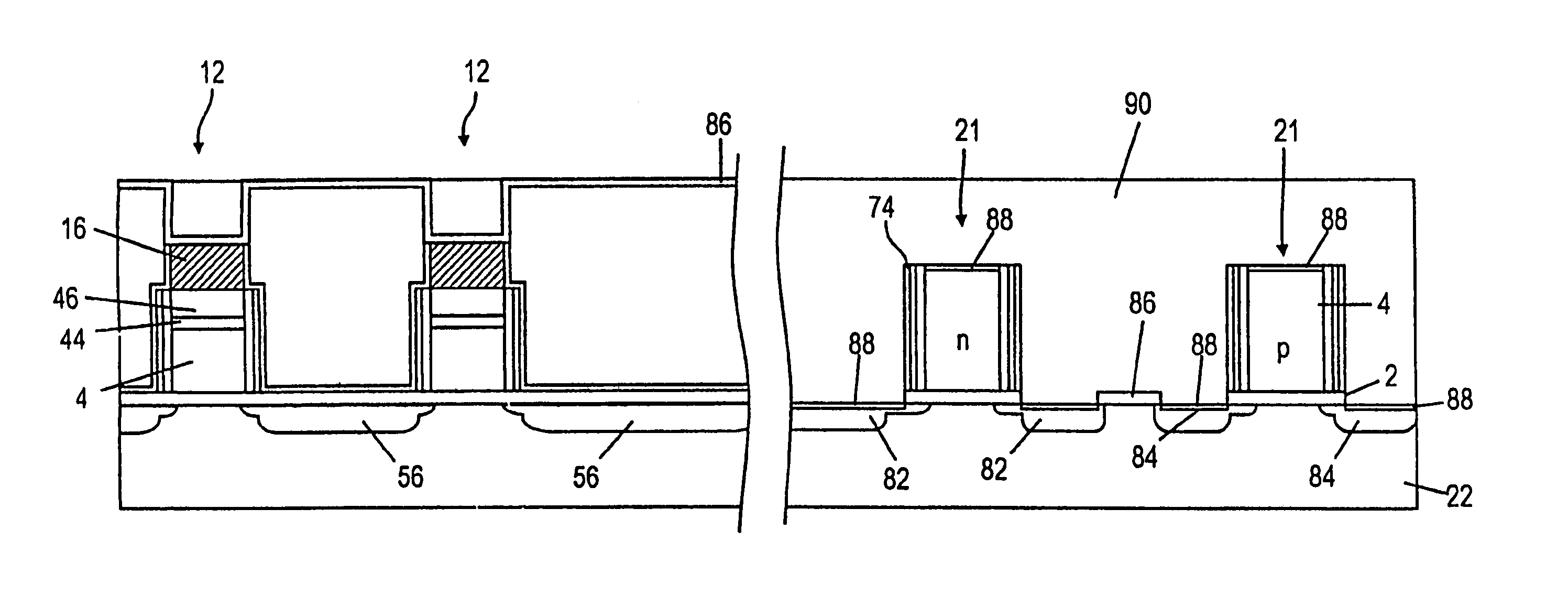
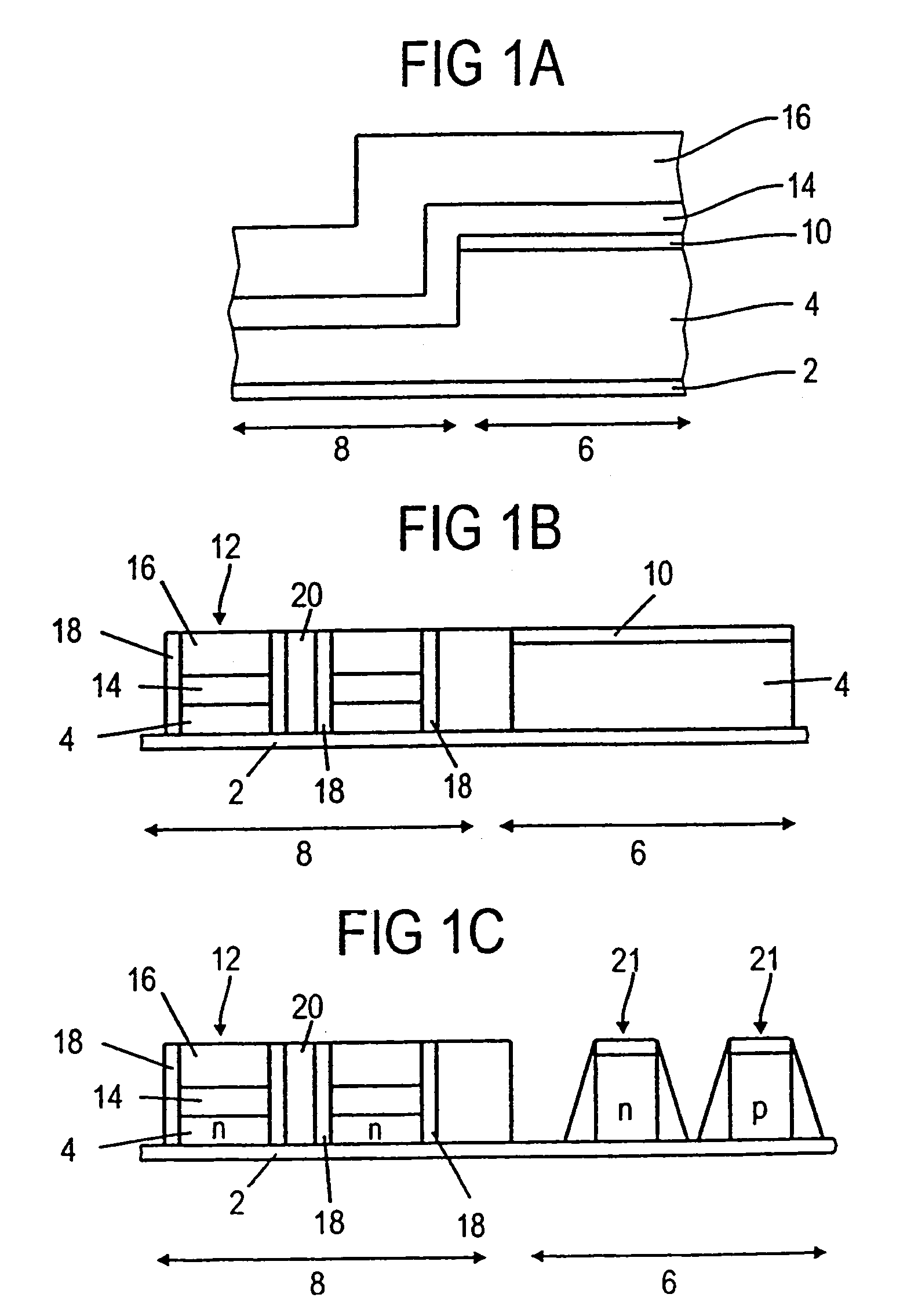
[0041]FIGS. 1A to 1C show the basic sequence of the method according to the invention. Firstly, a dielectric layer 2 and a semiconductor layer 4 are formed. The semiconductor layer 4 is made thicker in the logic region 6, lying in the right-hand half of the figure in FIG. 1A, than in the memory region 8, lying in the left-hand half of the figure. 10 designates an insulating layer which covers the semiconductor layer 4 in the logic region 6. Before the formation of the gate electrodes 12 in the memory region 8, a metal-including layer 14 and a covering insulation layer 16 are deposited over the whole area. The formation of the dielectric layer 2 is typically preceded by the formation of the wells for the transistors to be formed, in particular in the logic region 6, by implantation.

[0042]As can be seen from FIG. 1B, the gate electrodes 12 in the memory region 8 are fabricated, which are laterally covered by insulating edge webs 18. Before the filling of the interspaces between the ga...


PUM


Abstract

A method for the integration of field-effect transistors for memory and logic applications in a semiconductor substrate is disclosed. The gate dielectric and a semiconductor layer are deposited over the whole area both in the logic region and in the memory region. From these layers, the gate electrodes in the memory region are formed, the source and drain regions are implanted and the memory region is covered in a planarizing manner with an insulation material. Afterward, the gate electrodes are formed from the semiconductor layer and the gate dielectric in the logic region.

Description

CLAIM FOR PRIORITY[0001]This application claims priority to International Application No. PCT / EP02 / 08484, published in the German langague on Feb. 20, 2003, which claims the benefit of priority to German Application No. DE 101 37 678.2, filed in the German language on Aug. 1, 2001.TECHNICAL FIELD OF THE INVENTION[0002]The invention relates to semiconductor technology, and and in particular to a method for fabricating a semiconductor product with a memory region and a logic region, and to a semiconductor product.BACKGROUND OF THE INVENTION[0003]Semiconductor products are being fabricated with integrated memory and logic regions to an increasing extent. However, this makes particularly stringent requirements of the fabrication process, since different requirements are made of the field-effect transistors (FE transistors) in the memory and logic regions. Thus, by way of example, the FE transistors in the memory region, which generally serve there as selection transistors for assigned m...

Claims


Application Information

Patent Timeline
IPC IPC(8): H01L21/8238H01L27/108H01L21/8239H01L21/8242H01L27/105
CPCH01L27/105H01L27/10894H01L27/1052H01L27/10873H10B12/05H10B12/09H01L21/0332H01L21/0415H01L29/4234H01L2924/1306H10B99/00
Inventor GRAF, WERNERKIESLICH, ALBRECHT
Owner POLARIS INNOVATIONS
Learn More