Pendeoepitaxial methods of fabricating gallium nitride semiconductor layers on sapphire substrates, and gallium nitride semiconductor structures fabricated thereby

a gallium nitride and semiconductor layer technology, applied in semiconductor devices, semiconductor lasers, laser details, etc., can solve the problems of limiting the mass production of gallium nitride devices, low defect densities of gallium nitride semiconductor layers, and relatively high cost of silicon carbide substrates, etc., to achieve low defect densities, low cost, and high availability

Inactive Publication Date: 2007-05-15
NORTH CAROLINA STATE UNIV
View PDF31 Cites 4 Cited by
  • Summary
  • Abstract
  • Description
  • Claims
  • Application Information

AI Technical Summary

Benefits of technology

[0019]Accordingly, sapphire may be employed as a substrate for growing gallium nitride semiconductor layers that

Problems solved by technology

A major problem in fabricating gallium nitride-based microelectronic devices is the fabrication of gallium nitride semiconductor layers having low defect densities.
However, a major concern that may limit the mass production of gallium nitride devices is the growth of the gallium nitride layers on a silicon carbide substrate.
Notwithstanding silicon carbide's increasing commercial importance, silicon carb

Method used


Image

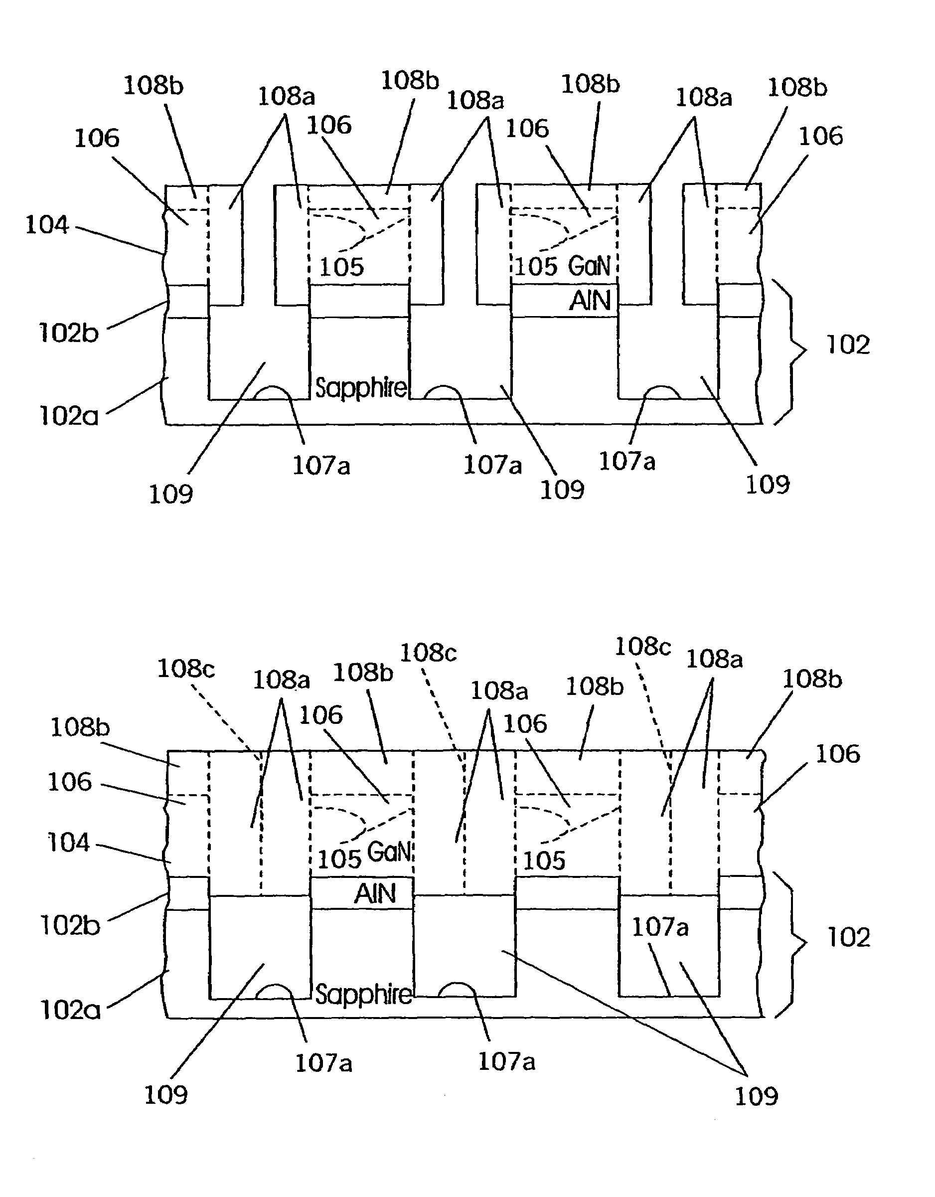
  • Pendeoepitaxial methods of fabricating gallium nitride semiconductor layers on sapphire substrates, and gallium nitride semiconductor structures fabricated thereby
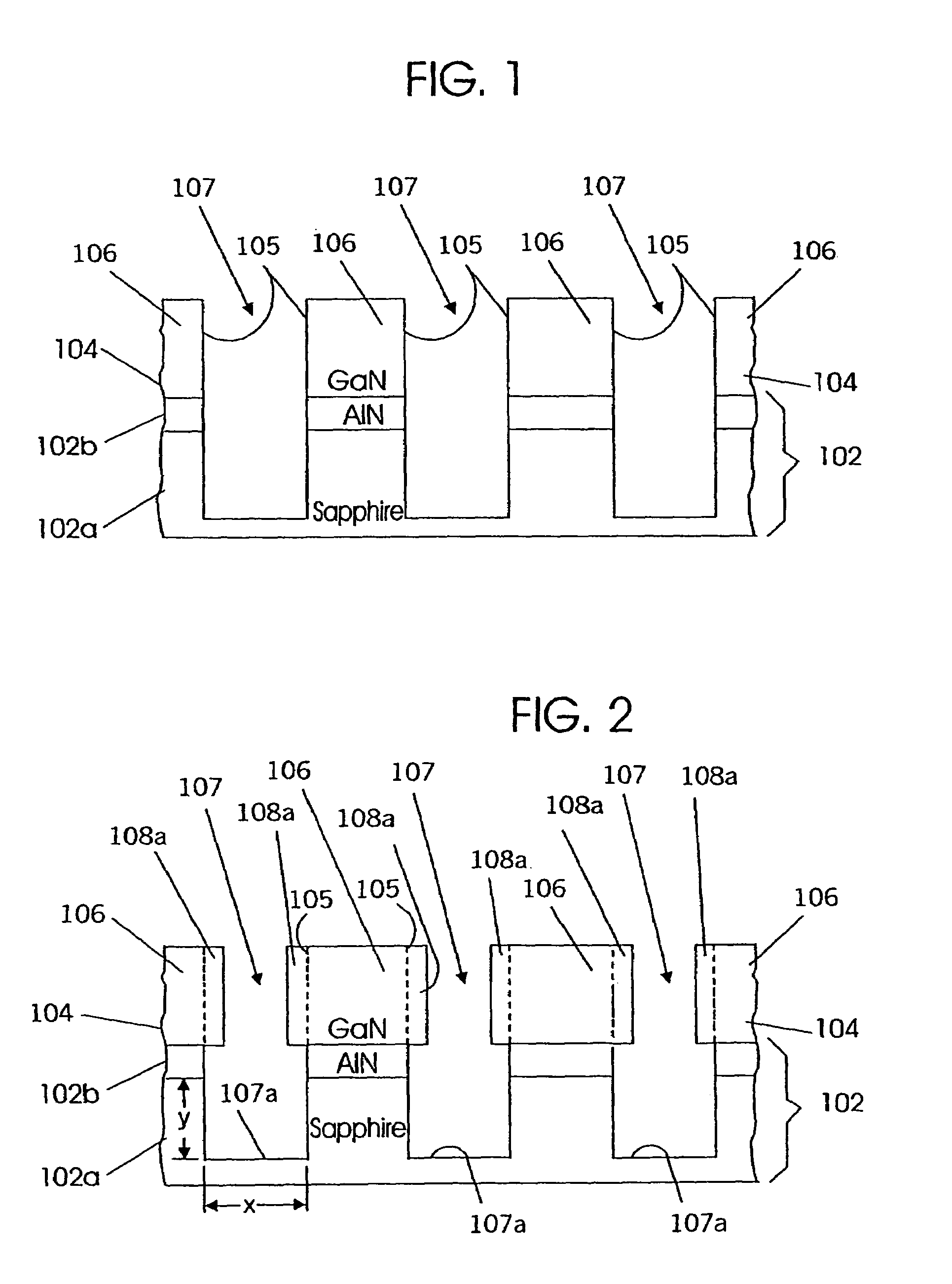
  • Pendeoepitaxial methods of fabricating gallium nitride semiconductor layers on sapphire substrates, and gallium nitride semiconductor structures fabricated thereby
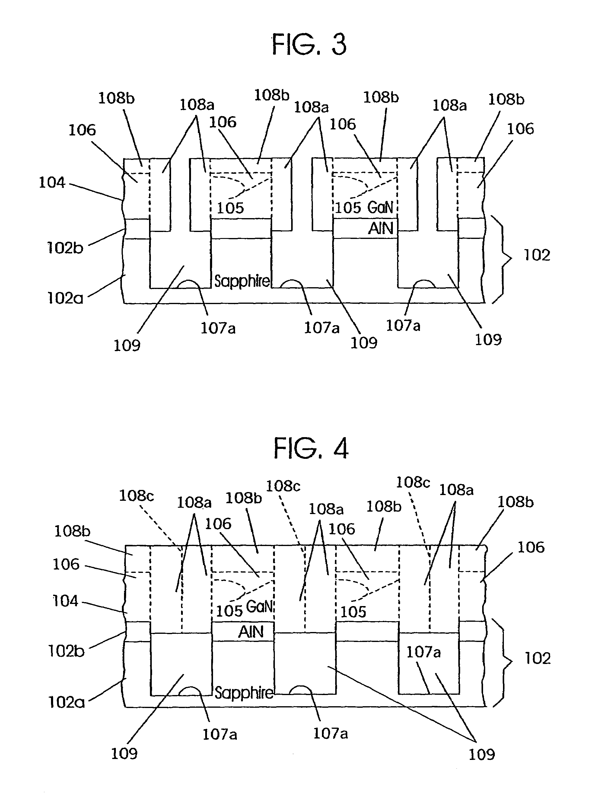
  • Pendeoepitaxial methods of fabricating gallium nitride semiconductor layers on sapphire substrates, and gallium nitride semiconductor structures fabricated thereby

Examples


Embodiment Construction

[0024]The present invention now will be described more fully hereinafter with reference to the accompanying drawings, in which preferred embodiments of the invention are shown. This invention may, however, be embodied in many different forms and should not be construed as limited to the embodiments set forth herein; rather, these embodiments are provided so that this disclosure will be thorough and complete, and will fully convey the scope of the invention to those skilled in the art. In the drawings, the thickness of layers and regions are exaggerated for clarity. Like numbers refer to like elements throughout. It will be understood that when an element such as a layer, region or substrate is referred to as being “on” or “onto” another element, it can be directly on the other element or intervening elements may also be present. Moreover, each embodiment described and illustrated herein includes its complementary conductivity type embodiment as well.

[0025]Referring now to FIGS. 1–5,...


PUM


Abstract

More specifically, gallium nitride semiconductor layers may be fabricated by etching an underlying gallium nitride layer on a sapphire substrate, to define at least one post in the underlying gallium nitride layer and at least one trench in the underlying gallium nitride layer. The at least one post includes a gallium nitride top and a gallium nitride sidewall. The at least one trench includes a trench floor. The gallium nitride sidewalls are laterally grown into the at least one trench, to thereby form a gallium nitride semiconductor layer. However, prior to performing the laterally growing step, the sapphire substrate and/or the underlying gallium nitride layer is treated to prevent growth of gallium nitride from the trench floor from interfering with the lateral growth of the gallium nitride sidewalls of the at least one post into the at least one trench. Embodiments of gallium nitride semiconductor structures according to the present invention can include a sapphire substrate and an underlying gallium nitride layer on the sapphire substrate. The underlying gallium nitride layer includes therein at least one post and at least one trench. The at least one post each includes a gallium nitride top and a gallium nitride sidewall. The at least one trench includes a sapphire floor. A lateral gallium nitride layer extends laterally from the gallium nitride sidewall of the at least one post into the at least one trench. In a preferred embodiment, the at least one trench extends into the sapphire substrate such that the at least one post each includes a gallium nitride top, a gallium nitride sidewall and a sapphire sidewall and the at least one trench includes a sapphire floor. The sapphire floor preferably is free of a vertical gallium nitride layer thereon and the sapphire sidewall height to sapphire floor width ratio preferably exceeds about 1/4. A mask may be included on the sapphire floor and an aluminum nitride buffer layer also may be included between the sapphire substrate and the underlying gallium nitride layer. A mask also may be included on the gallium nitride top.

Description

CROSS REFERENCE TO RELATED APPLICATION[0001]This application is a continuation of and claims priority from U.S. patent application Ser. No. 10 / 404,616, now issued U.S. Pat. No. 6,686,261, filed Apr. 1, 2003, which in turn is a continuation application of, and claims priority from, U.S. patent application Ser. No. 09 / 899,586 filed Jul. 3, 2001, now issued U.S. Pat. No. 6,545,300, which in turn is a divisional application and claims priority from, U.S. patent application Ser. No. 09 / 441,753, filed Nov. 17, 1999, now issued U.S. Pat. No. 6,521,514, the entire disclosures of which are incorporated herein by reference.FEDERALLY SPONSORED RESEARCH[0002]This invention was made with Government support under Office of Naval Research Contract Nos. N00014-96-1-0765, N00014-98-1-0384, and N00014-98-1-0654. The Government may have certain rights to this invention.FIELD OF THE INVENTION[0003]This invention relates to microelectronic devices and fabrication methods, and more particularly to galliu...

Claims


Application Information

Patent Timeline
IPC IPC(8): H01L21/84H01L21/336H01L29/205H01L21/20H01L21/205H01S5/02H01S5/323
CPCH01L21/0242H01L21/02458H01L21/0254H01L21/0262H01L21/02639H01L21/02642H01L21/02647H01L21/0265H01S5/0213H01S2304/12
Inventor GEHRKE, THOMASLINTHICUM, KEVIN J.DAVIS, ROBERT F.
Owner NORTH CAROLINA STATE UNIV
Why Eureka
Try Eureka