Metallic nanowire interconnections for integrated circuit fabrication

a technology of integrated circuit fabrication and nanowires, which is applied in the direction of electrical equipment, semiconductor devices, semiconductor/solid-state device details, etc., can solve the problems of high resistance to electrical migration material and processing difficulties, and increased resistance of common interconnect metals to electro-migration

Inactive Publication Date: 2007-05-15
NASA
View PDF24 Cites 35 Cited by
  • Summary
  • Abstract
  • Description
  • Claims
  • Application Information

AI Technical Summary

Problems solved by technology

Microprocessors require local, intermediate and global wiring solutions and present both material and processing difficulties.
Susceptibility of common interconnect metals to electro-migration at high current densities (above 106 Amp / cm2) is a problem.
However, electrical resistivity of copper increases with decreasing dimensions and is attributed to scattering at surfaces and at grain boundaries.
These size effects are due to interface roughness and through use of small grain sizes, which are hard to overcome and cannot be avoided by simply cooling to lower the resistivity.
Creating high aspect ratio apertures with straight walls and uniform diameters using dry etching is an extremely difficult task and is expected to become progressively more difficult with each succeeding generation.
Aspect ratio-dependent etching becomes a serious problem with each new decrease in feature size.
Plasma damage and cleaning of high aspect ratio features also pose concerns.
Cleaning a trench after its creation is also a problem, in part because of the shrinking width of the trench.
Filling a deep, narrow trench with an interconnect metal, in a manner that does not create voids, is also becoming a problem.

Method used


Image

  • Metallic nanowire interconnections for integrated circuit fabrication
  • Metallic nanowire interconnections for integrated circuit fabrication
  • Metallic nanowire interconnections for integrated circuit fabrication

Examples


Embodiment Construction

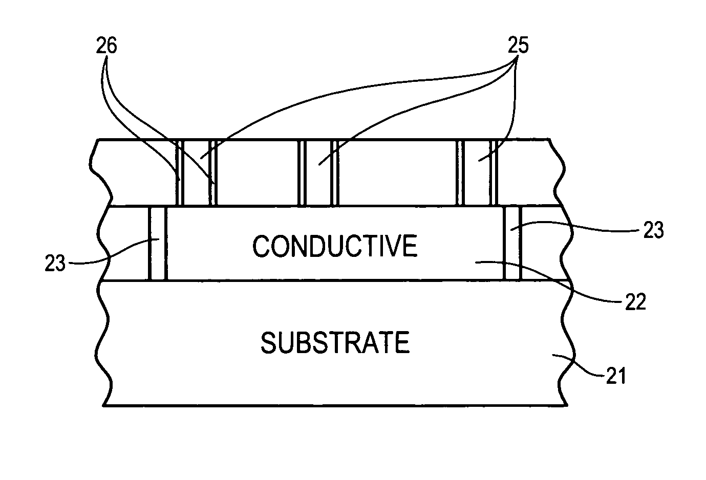
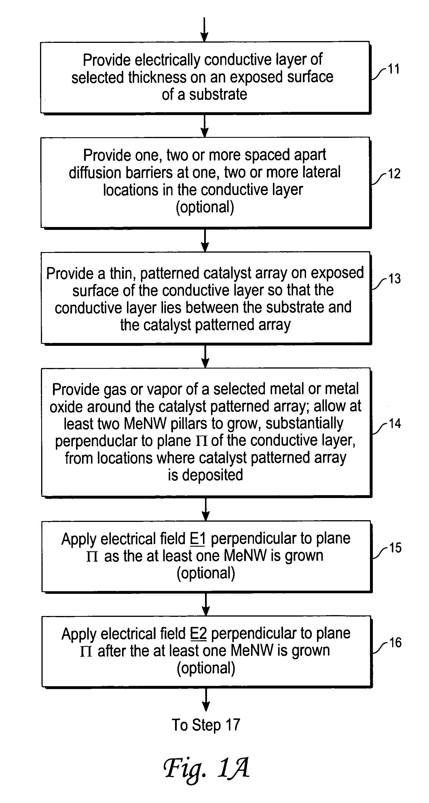
[0016]FIG. 1A / 1B is a flow chart of a procedure for practicing the invention. In step 11 (illustrated in FIG. 2A), an electrically conductive layer 22, preferably having a thickness in the range 0.2–250 nm, is provided on an exposed surface of a substrate 21, which may have any reasonable thickness. The substrate material may be silicon or a silicon on insulator, and the conductive layer material may be Cu, Ag, Au, Pd, Pt, Ni, Fe, Co, Ir, Ti, Zr, and / or a metal-doped silicide. Optionally, two or more spaced apart diffusion barriers 23 of a selected barrier material (e.g., TiuNv or TauNv of thickness 1–10 nm, where u and v are positive numbers) is provided at one, two or more laterally displaced locations in the conductive layer 22, to limit transverse movement of the conductive layer material, in step 12.

[0017]In step 13 (illustrated in FIG. 2B), a thin, patterned array 24 of MeNW catalyst elements, preferably having thicknesses of 0.1–20 nm, is provided on an exposed surface of the...


PUM

PropertyMeasurementUnit
thicknessaaaaaaaaaa
thicknessaaaaaaaaaa
diameteraaaaaaaaaa

Abstract

A method for fabricating an electrical interconnect between two or more electrical components. A conductive layer is provided on a substarte and a thin, patterned catalyst array is deposited on an exposed surface of the conductive layer. A gas or vapor of a metallic precursor of a metal nanowire (MeNW) is provided around the catalyst array, and MeNWs grow between the conductive layer and the catalyst array. The catalyst array and a portion of each of the MeNWs are removed to provide exposed ends of the MeNWs.

Description

CROSS REFERENCE TO RELATED APPLICATIONS[0001]This application is a Continuation In Part of, and claims the benefit of, a patent application, U.S. Ser. No. 10 / 390,254, filed Mar. 11, 2003 now U.S. Pat. No. 7,094,674.ORIGIN OF THE INVENTION[0002]The invention described herein was made by employees of the United States Government and may be manufactured and used by or for the Government for governmental purposes without the payment of any royalties thereon or therefor.TECHNICAL FIELD[0003]The present invention is a method for providing electrical interconnects for integrated circuit fabrication.BACKGROUND OF THE INVENTION[0004]An interconnect in an integrated circuit (IC) distributes clock, regulatory and other signals as well as power or ground voltages to various components and circuits on a chip. The International Technology Roadmap for Semiconductors (ITRS) emphasizes the high speed transmission requirements on a chip as the driver for future interconnect development. Near term and...

Claims


Application Information

Patent Timeline
Patent Type & Authority Patents(United States)
IPC IPC(8): H01L21/4763
CPCH01L21/76885H01L23/53276H01L2221/1094Y10S977/843H01L2924/0002Y10S977/842H01L2924/00
Inventor NG, HOU TEELI, JUNMEYYAPPAN, MEYYA
Owner NASA
Why Eureka
Try Eureka