Low temperature process and structures for polycide power MOSFET with ultra-shallow source

a polycide power mosfet, low temperature technology, applied in the direction of semiconductor devices, electrical equipment, transistors, etc., can solve the problems of high diffusion temperature and/or process time, increased temperature and process time generally affecting device performance, affecting device performance, etc., to reduce the vertical depth

Active Publication Date: 2007-05-15
INFINEON TECH AMERICAS CORP
View PDF13 Cites 4 Cited by
  • Summary
  • Abstract
  • Description
  • Claims
  • Application Information

AI Technical Summary

Benefits of technology

[0013]Accordingly, it would be desirable to produce a trench type power semiconductor device that has source regions with reduced vertical depth, thereby overcoming the above and other disadvantages of the prior art. In accordance with the present invention, a trench type power MOSFET has “proud” gate electrodes that extend out of the trenches and above the surface of the semiconductor body. These proud gate electrodes enable making ultra-shallow source regions with nano-scale dimensions within the semiconductor body using a lower temperature source drive. Specifically, because the gate electrodes extend above the surface of the semiconductor body, there is no longer a need to diffuse the source regions to a depth that ensures vertical overlap to the gates and as such, the gate electrodes can be made ultra-shallow. In particular, the source regions of the present invention have vertical depths that are approximately equal to or less than the thickness of the gate oxide that lines the trenches of the device.
[0015]The ultra-shallow source regions of the present invention have several advantages. For example, the reduced temperatures that can be used to form the source regions allows for an improved fabrication process where all process steps following the formation of gate electrodes within the trenches of the MOSFET device can be preformed at temperatures below 900° C. In addition, the formation of ultra-shallow source regions also results in source regions with less lateral diffusion. By reducing the lateral diffusion of the source regions, the distance between trenches can be reduced, thereby increasing the cell density of the device and the current the device can handle. Furthermore, because of the ultra-shallow source regions, the vertical depth of the channel region of the device can be reduced, thereby reducing the length of the trenches and reducing the length of the gate electrodes. The reduced gate electrode lengths decreases gate charge (Qg) and improves the efficiency of the device.
[0016]In accordance with another aspect of the invention, the power MOSFET may optionally include silicide / salicide contacts on the gate electrodes, thereby reducing the resistive value (Rg) of the electrodes. In accordance with a further aspect of the invention, the power MOSFET includes high conductivity contact regions adjacent to the source regions and may optionally include silicide / salicide contacts that short the source regions to the high conductivity contact regions. These silicide / salicide contacts both reduce the contact resistance between the source regions and the source electrode of the device, thereby reducing the device's on-state resistance (RDS(on)), and also improves the device's avalanche performance.

Problems solved by technology

For example, larger vertical diffusions require higher diffusion temperatures and / or process times. However, increased temperatures and process times will generally affect fabrication costs and / or affect device performance.
For example, high temperature process steps can adversely affect previously performed low temperature steps.
Alternatively, for example, the high temperature steps must be performed at reduced temperatures but at the cost of increased process times.
Another problem with larger vertical diffusions for source regions is that dopants do not only move vertically, but also laterally during diffusion.
However, this lateral diffusion is generally undesirable because it means the distance between trenches has to be increased.
Increasing the distance between adjacent trenches, however, increases cell size.
A further problem with larger vertical diffusions for source regions is that as the vertical depth of the source regions increases, the vertical depth of channel region 20 into epitaxial silicon layer 16 must also increase.

Method used


Image

  • Low temperature process and structures for polycide power MOSFET with ultra-shallow source
  • Low temperature process and structures for polycide power MOSFET with ultra-shallow source
  • Low temperature process and structures for polycide power MOSFET with ultra-shallow source

Examples


Embodiment Construction

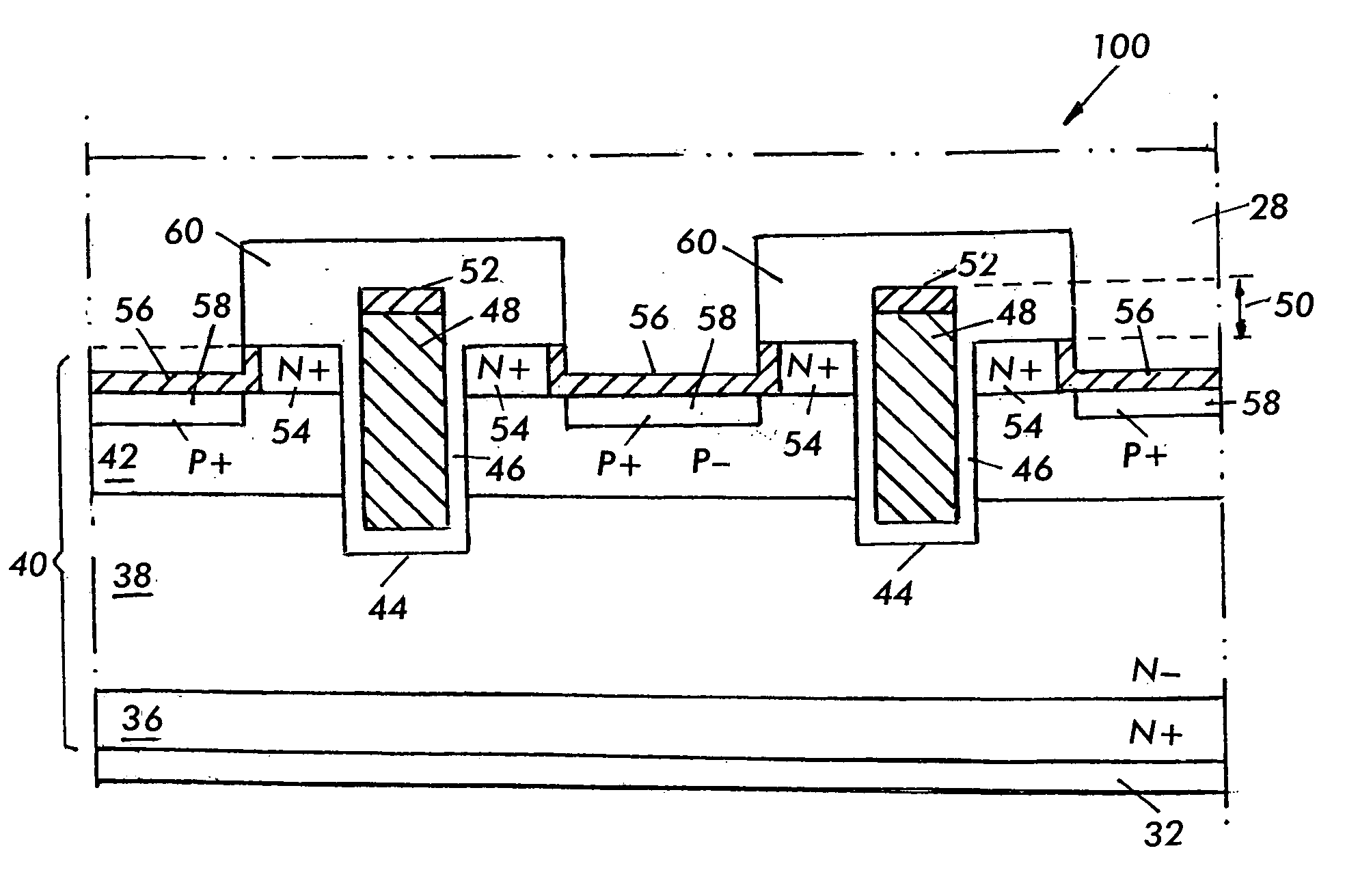
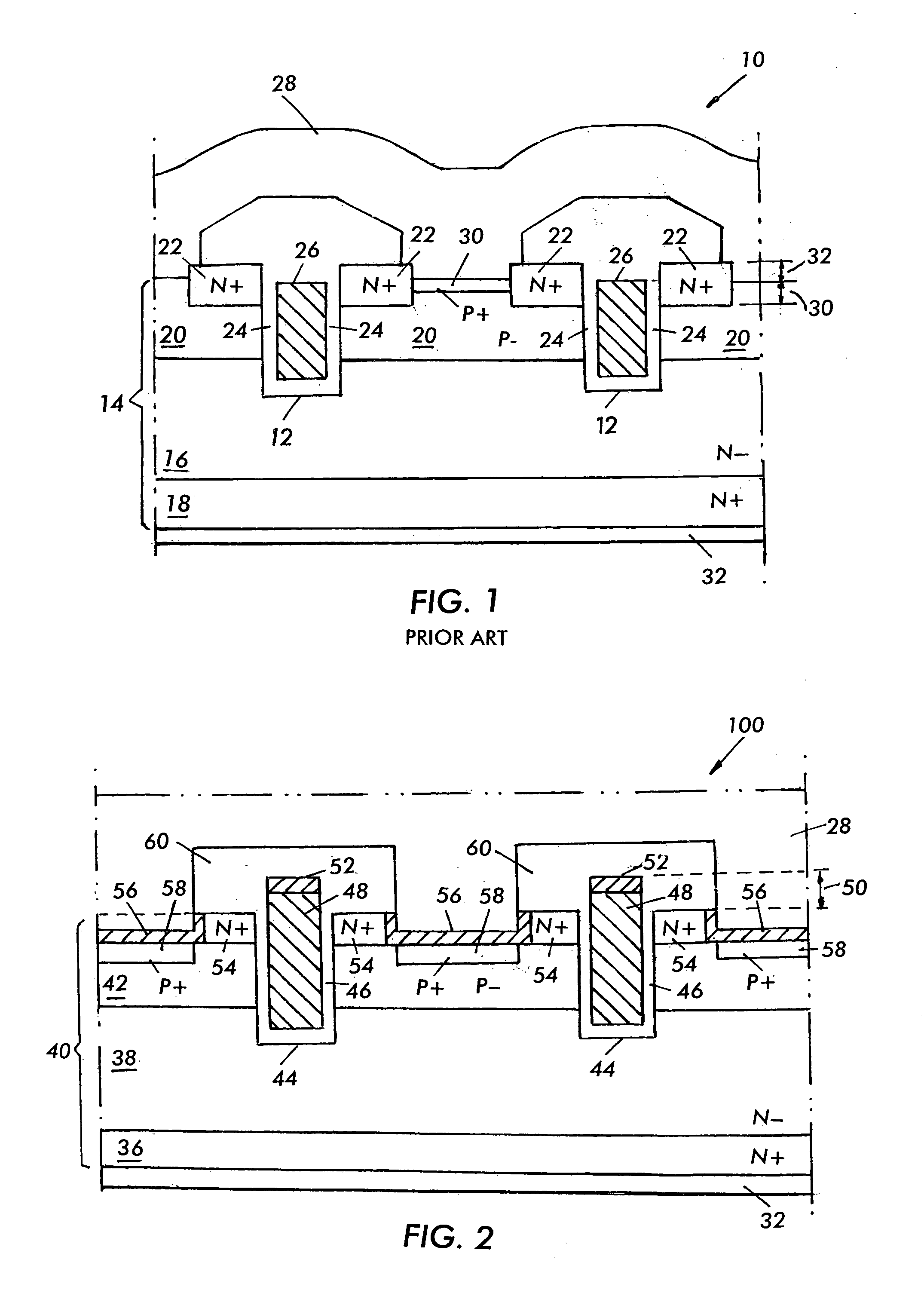
[0021]Referring to FIG. 2, a section of an example power MOSFET 100 according to an embodiment of the present invention is illustrated. MOSFET 100 comprises a semiconductor body 40, which includes silicon substrate 36 and epitaxial silicon layer 38. Silicon substrate 36 and epitaxial silicon layer 38 have the same conductivity (e.g., N-type), with epitaxial silicon layer 38 including a lower concentration of dopants as compared to substrate 36. Semiconductor body 40 also includes channel region 42, which has conductivity opposite to that of epitaxial silicon layer 38 (e.g. P-type).

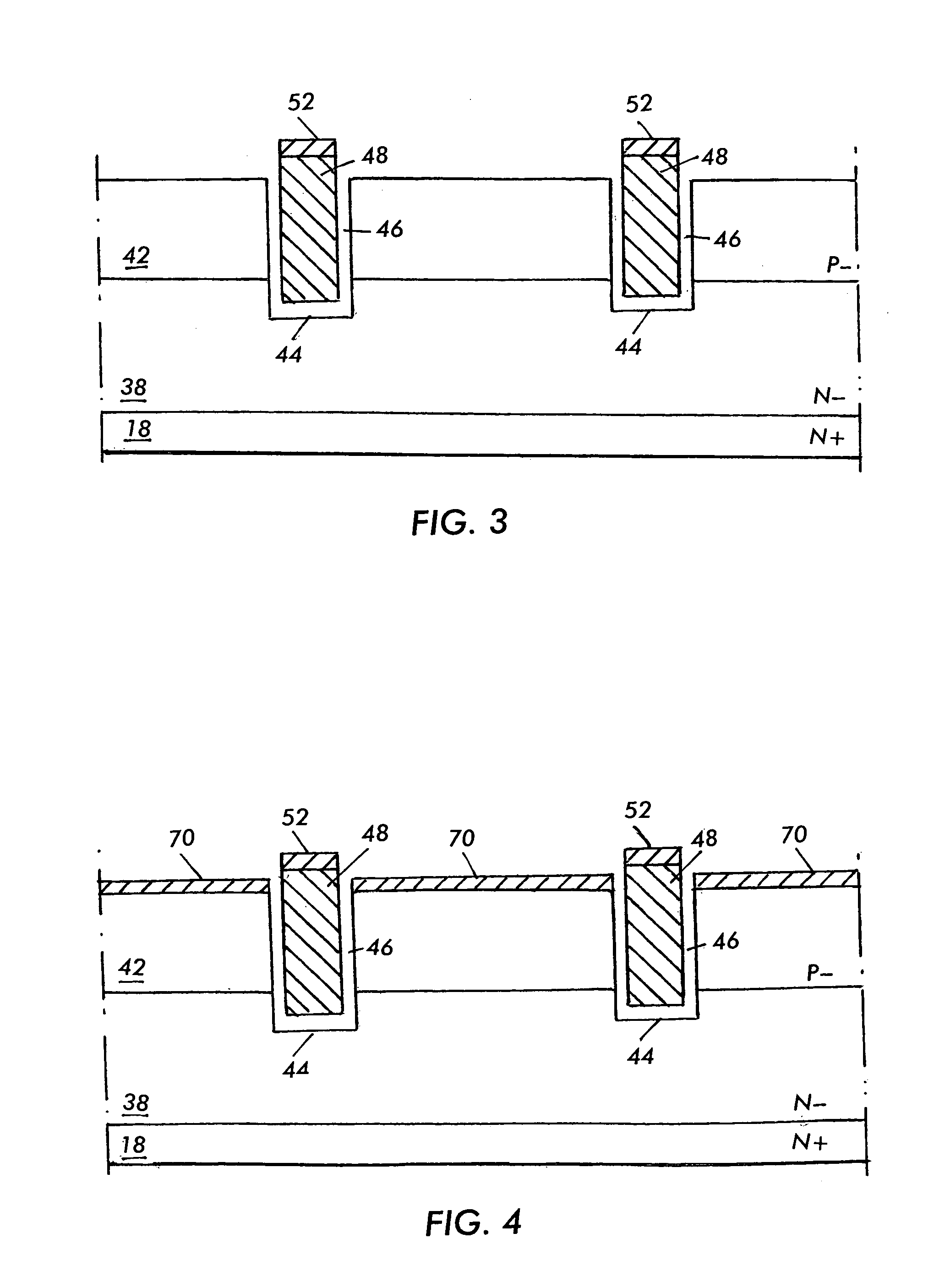
[0022]Formed within semiconductor body 40 are a plurality of trenches 44. Each of these trenches is lined with a gate insulation layer 46, formed with silicon dioxide, for example. Within each trench 46 are gate electrodes 48, composed of conductive polysilicon, for example. Significantly and as further discussed below, gate electrodes 48 are “proud”, that is, the gate electrodes extend out of trenches 44 ...


PUM


Abstract

A trench type power semiconductor device includes proud gate electrodes that extend out of the trenches and above the surface of the semiconductor body. These proud gate electrodes allow for making ultra-shallow source regions within the semiconductor body using, for example, a low temperature source drive. In addition, a method for manufacturing the trench type power semiconductor device includes a low temperature process flow once the gate electrodes are formed.

Description

RELATED APPLICATIONS[0001]This application is based on and claims priority to U.S. Provisional Application No. 60 / 543,440, filed on Feb. 9, 2004, by Kyle Spring, entitled, “Low Temperature Process and Structures For Polycide Power MOSFET with Ultra Shallow Source,” the contents of which are herein incorporated by reference.[0002]This application is also related to U.S. patent application Ser. No. 10 / 981,114, filed Nov. 4, 2004, by Kyle Spring, Jianjun Cao, Paul Harvey, Dave Kent, Robert Montgomery, and Hugo Burke, entitled “Trench Power MOSFET with Reduced Gate Resistance,” the contents of which are herein incorporated by reference.BACKGROUND OF THE INVENTION[0003]1. Field of the Invention[0004]The present invention relates generally to MOSFET devices, and more specifically, to trench-type MOSFET devices with ultra-shallow source regions and low temperature process flows.[0005]2. Description of Related Art[0006]Trench type power semiconductor devices such as power MOSFETs are well k...

Claims


Application Information

Patent Timeline
Patent Type & Authority Patents(United States)
IPC IPC(8): H01L29/76H01L29/94H01L31/062H01L31/113H01L31/119H01L21/336H01L29/45H01L29/49H01L29/78H01L29/788
CPCH01L29/4236H01L29/4933H01L29/66727H01L29/66734H01L29/7813H01L29/456
Inventor SPRING, KYLE
Owner INFINEON TECH AMERICAS CORP
Why Eureka
Try Eureka