Optical deflector

a technology of optical deflector and movable portion, which is applied in the direction of optical elements, mountings, instruments, etc., can solve the problems of reducing the deflection angle of a movable portion, affecting the operation of the deflector, so as to reduce the structural size, reduce the driving voltage, and reduce the deflection angl

Inactive Publication Date: 2007-05-22
CANON KK
View PDF23 Cites 29 Cited by
  • Summary
  • Abstract
  • Description
  • Claims
  • Application Information

AI Technical Summary

Benefits of technology

[0012]In a third structure, the first support portion is comprised of a pair of torsion bars for rotatably supporting the movable mirror in a torsional-vibration manner about the first rotational axis relative to the gimbal, and the second support portion is comprised of a pair of torsion bars for rotatably supporting the gimbal in a torsional-vibration manner about the second rotational axis relative to the frame. When such torsion bars are used, it is possible to readily achieve resonance driving and high-speed scanning. However, any type of a support portion can be used so long as the movable mirror and the gimbal can be rotatably supported. Further, the first rotational axis of the movable mirror can form any angle, such as right angles, relative to the second rotational angle of the gimbal.
[0013]In a fourth structure, the electromagnetic driving unit includes a stationary coil and a movable magnet disposed on the movable mirror, and the movable mirror is displaced by an electromagnetic force acting between the stationary coil and the movable magnet. Alternatively, in a fifth structure, the electromagnetic driving unit includes at least a stationary magnet and a movable coil disposed on the movable mirror, and the movable mirror is displaced by an electromagnetic force acting between the stationary magnet and the movable coil. In this structure, a plurality of stationary magnets can be discretely arranged in a row parallel to the second rotational axis of the gimbal. With such an arrangement, a large deflection angle of the gimbal can be achieved.
[0017]According to the present invention, it is possible to provide an optical deflector with a two-axis driving gimbal structure, in which a deflection angle of a movable portion can be made relatively large, a driving voltage for driving a movable portion can be made relatively low, a structural size can be reduced, high-speed scanning can be carried out, and crosstalk between driving signals for the two rotational axes can be reduced.
[0018]More specifically, the deflection angle can be made relatively large because of the electrostatic driving using the movable and stationary comb electrodes, which face each other at their planar surfaces extending approximately parallel to the direction of the rotational movement of the gimbal. Also, the driving voltage can be made relatively low because of the electromagnetic driving for displacing the movable mirror by the electromagnetic force, and the structural size can be reduced because of the use of such electrostatic driving and electromagnetic driving. Further, high-speed scanning can be achieved because the movable mirror is electromagnetically driven such that its moment of inertia can be comparatively decreased, and the crosstalk can be reduced because of properties of driving forces for rotations about the two axes (the first and second rotational axes) are made different from each other.
[0019]Further, when the recess portion is formed on the common substrate, it is possible to improve a positional precision of the stationary comb electrode, the stationary coil, or the stationary magnet placed at the recess portion. When a plurality of the stationary magnets are discretely arranged in a row parallel to the second rotational axis of the gimbal, both deflection angles about the first and second rotational axes can be increased.
[0020]Furthermore, according to the present invention, it is possible to achieve an image forming apparatus in which a structural size can be reduced, a driving voltage can be made relatively low, a deflection angle can be made relatively large, and a highly-precise image can be obtained.

Problems solved by technology

Therefore, the problem of crosstalk between electric fields generated by the two sets of electrodes is likely to occur, irrespective of the type of the electrodes (i.e., flat opposed electrodes, interdigitated comb electrodes, or the like).
Accordingly, problems of restriction of arrangement of the magnets and crosstalk between magnetic fields generated by the two sets of permanent magnets and electromagnetic coils are likely to occur, irrespective of the type of the electromagnetic driving (i.e., the moving magnet type, the moving coil type, or the like).
Further, in a case where one drive is carried out in an electrostatic manner using the flat opposed electrode, one of power generated for driving the movable portion and the displacement amount of the movable portion must be restricted owing to a structural disadvantage of the flat opposed electrode.
In other words, if an inter-electrode distance (a distance between the flat opposed electrodes) is enlarged to achieve a large displacement amount of the movable portion, a driving voltage for achieving a desired displacement angle of the movable portion must be unavoidably increased.

Method used


Image

  • Optical deflector
  • Optical deflector
  • Optical deflector

Examples


first embodiment

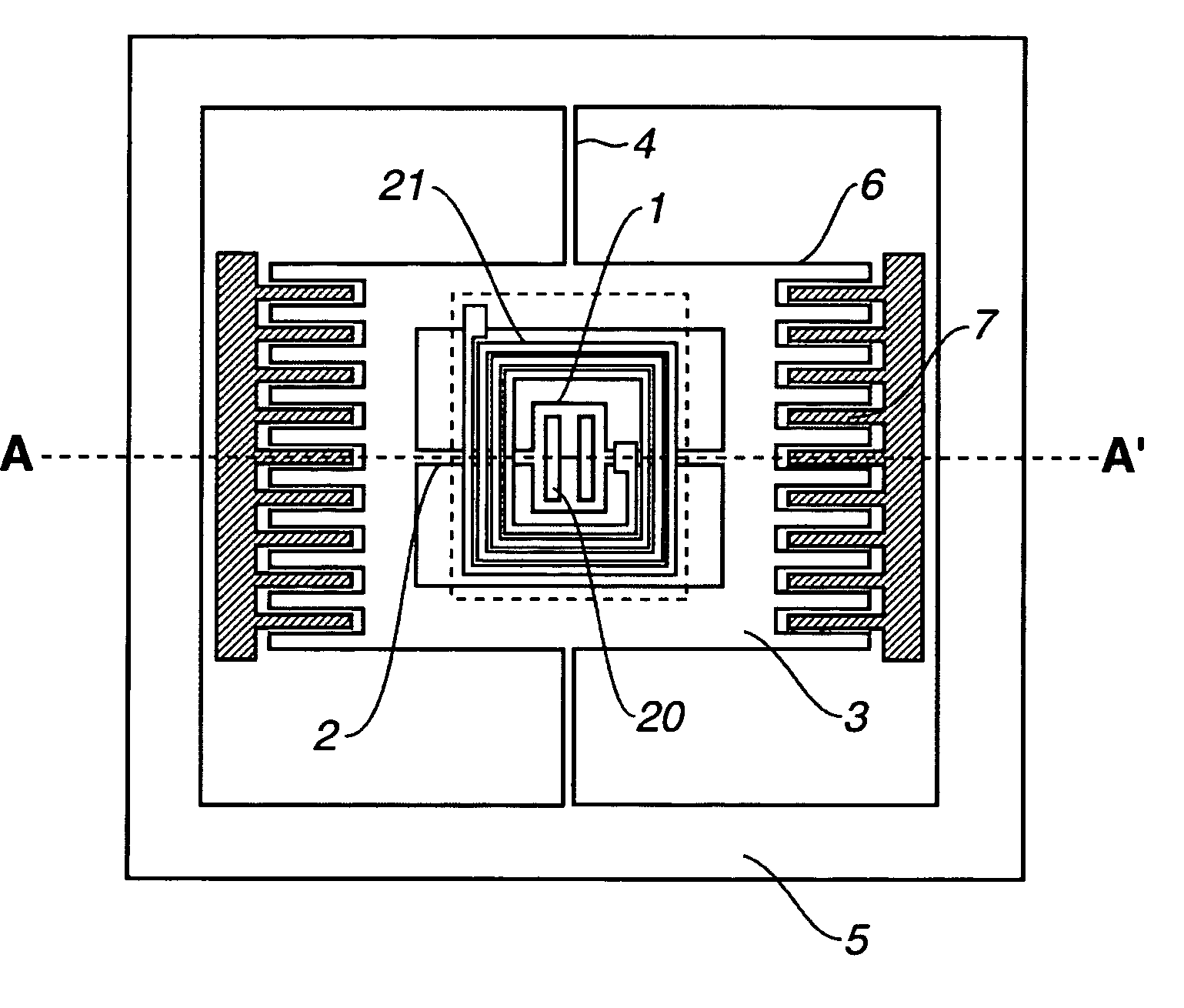
[0041]an optical deflector will be first described with reference to FIGS. 6A and 6B, and FIGS. 7A to 7C. In those figures, reference numeral 1 designates a movable mirror, reference numerals 2 and 4 designate torsion bars, reference numeral 3 designates a gimbal or a movable frame, reference numeral 5 designates a frame, reference numeral 6 designates a movable interdigitated comb electrode, reference numeral 7 designates a stationary interdigitated comb electrode, reference numeral 8 designates a pull-out electrode for pulling out the stationary interdigitated comb electrode 7, reference numeral 9 designates a common substrate, reference numeral 10 designates a spacer, reference numeral 11 designates a reflective film, reference numeral 20 designates a movable magnet, reference numeral 21 designates a stationary coil, reference numeral 22 designates a coil substrate, and reference numeral 23 designates a pull-out electrode for pulling out the stationary coil 21.

[0042]In the first ...

fourth embodiment

[0050]the image forming apparatus will be described with reference to FIG. 10. In FIG. 10, reference numeral 51 designates a driving portion for modulating a light source, reference numeral 52 designates a modulation signal, reference numeral 53 designates a light source to be directly modulated, reference numeral 54 designates directly-modulated output light, reference numeral 55 designates an optical deflector of the present invention, reference numeral 56 designates a correction optical system, and reference numeral 57 designates an image display member.

[0051]In this image forming apparatus, the optical deflector 55 used herein have technical advantages that the driving voltage can be made relatively low, that a high-speed scanning can be carried out, and that the deflection angle can be made relatively large. Therefore, in the image forming apparatus using the optical deflector 55, its cost and size can be reduced, the electrical power consumption can be lowered, and the resolut...

second embodiment

[0063]A second example of the optical deflector will be described with reference to FIGS. 8A and 8B. Its schematic construction is described in the second embodiment, and the structure of the second example is approximately the same as that of the first example.

[0064]The second example is different from the first example in that the stationary interdigitated comb electrodes 7 and the coil substrate 22 are placed on the recess portions 25 formed on the common substrate 9, respectively, as illustrated in FIGS. 8A and 8B. The recess portion 25 can be precisely formed on the common substrate 9 by photolithography and etching. In the second example, a single crystal silicon substrate with a (100) face is used as the common substrate 9, and the recess portion 25 having a depth of 200 microns is formed using 30%-water solution of potassium hydroxide heated to 100° C.

[0065]In the second example, the stationary interdigitated comb electrodes 7 and the coil substrate 22 are placed on the rece...


PUM


Abstract

The present invention provides a resonance type micro-oscillating member capable of retraining a fluctuation of angular velocity, and specifically provides a micro-oscillating member, which is a nested micro-oscillating member, wherein there exist a reference oscillation mode which is the characteristic oscillation mode of a reference frequency, and an even numbered oscillation mode which is the characteristic oscillation mode of a frequency being approximate even number times the reference frequency.

Description

BACKGROUND OF THE INVENTION[0001]1. Field of the Invention[0002]The present invention relates to an optical deflector capable of being fabricated by techniques of micromechanics or the like.[0003]2. Description of the Related Background Art[0004]In recent years, development of a microactuator, using techniques of micromechanics has been energetically advanced. Electrostatic driving, piezoelectric driving, electromagnetic driving and the like can be employed as its driving means. A small-sized large-output (i.e., a relatively large deflection angle can be obtained by a relatively small electrical power) microactuator is increasingly required as demands for reduction in its cost, its application to mobile equipment, and the like increase. Particularly, an optical deflector for deflecting a movable mirror supported with a couple of torsion bars has been increasingly developed as a device capable of achieving a relatively simple optical sensor, an image forming apparatus, or the like.[0...

Claims


Application Information

Patent Timeline
Patent Type & Authority Patents(United States)
IPC IPC(8): G02B5/08B41J2/44B81B3/00G02B26/08G02B26/10H04N1/036H04N1/113
CPCG02B26/0841G02B26/085
Inventor SHIMADA, YASUHIROKATO, TAKAHISA
Owner CANON KK
Why Eureka
Try Eureka