Receiver circuit and radio communication terminal apparatus

a technology of reception circuit and reception circuit, which is applied in the direction of gain control, dc level restoring means or bias distort correction, baseband system details, etc., can solve the problems of low input tolerance of lna itself, low gain, and circuit saturation caused by desired signal, etc., to save the area occupied by inductive elements, the chip unit price becomes lower, and the die size is reduced

Active Publication Date: 2007-05-22
SNAPTRACK
View PDF9 Cites 52 Cited by
  • Summary
  • Abstract
  • Description
  • Claims
  • Application Information

AI Technical Summary

Benefits of technology

[0011]In this reception circuit, it is preferable that, during operation of the above-mentioned low noise amplifying circuit with the high gain, its DC bias current is passed independently of a DC bias current of the above-mentioned quadrature demodulator, and during operation of the above-mentioned low noise amplifying circuit with the low gain, its DC bias current is shared with a DC bias current of the above-mentioned quadrature demodulator. Thus, consumed power in the reception circuit is reduced when the low noise amplifying circuit with the low gain is selected for operation.
[0013]It is possible to provide a configuration in which the above-mentioned first to fourth inductive elements are formed of a single inductor in which a spiral is smaller helically from a first terminal in an outermost portion and then the spiral is larger through gaps of the helicity, and returns to a second terminal in the outermost portion, and a third and a fourth terminals are drawn from two positions in the middle between an innermost portion of the inductor and the above-mentioned first and second terminals, a fifth terminal is drawn from a position in the innermost portion, the above-mentioned first and second terminals are connected to the emitters of the pair of transistors in the above-mentioned low noise amplifying circuit with the low gain, the above-mentioned third and fourth terminals are connected to the emitters of the pair of transistors in the above-mentioned low noise amplifying circuit with the high gain, and the above-mentioned fifth terminal is grounded through a resistance. Thus, the area occupied by the first to fourth inductive elements is reduced when the reception circuit is formed as an IC chip.
[0015]With this configuration, in a state in which it is close to a base station, that is, when a reception signal level is higher than a predetermined level, the LNA is set to the low gain to realize low power consumption. If the reception signal predetermined level with which the LNA is switched to the low gain is set to be equal to or lower than average reception power of the terminal, average power consumption of the terminal is reduced. In addition, in a state in which the wireless communication terminal is far from a base station, that is, when a reception signal level is lower than the predetermined level, the LNA is set to the high gain, and in this event, the LNA is coupled with a direct capacitance to the quadrature demodulator, thereby making it possible to remove a second-order distortion component produced in the LNA to prevent it from being input to the quadrature demodulator.
[0017]In addition, the first to fourth inductive elements in the two LNA with different gains are formed of the single symmetrical type inductor to allow saving of the area occupied by the inductive elements on the chip. As a result, a die size becomes reduced and a chip unit price becomes lower.

Problems solved by technology

On the other hand, when a desired reception signal level is high, the interference due to the TX leakage mentioned above can be ignored, but on the contrary, circuit saturation caused by the desired signal presents a problem.
In this case, there is a problem that, although the level of a signal input to a later stage is reduced, high input tolerance of the LNA itself (such as IIP3 (3 order Input Intercept Point)) is not improved.
However, in this circuit scheme, there is a problem that, since the input is only attenuated, a high gain is not provided and gain arrangement has no flexibility.
Specifically, a through path in which the switches SW3 and SW4 are turned on includes an insertion loss of the switch and a mismatching loss of a matching circuit, and this configuration has no active circuit and thus a positive gain cannot be provided.

Method used


Image

  • Receiver circuit and radio communication terminal apparatus
  • Receiver circuit and radio communication terminal apparatus
  • Receiver circuit and radio communication terminal apparatus

Examples


Embodiment Construction

[0027]In the following, an embodiment of the present invention will be described in detail with reference to the drawings.

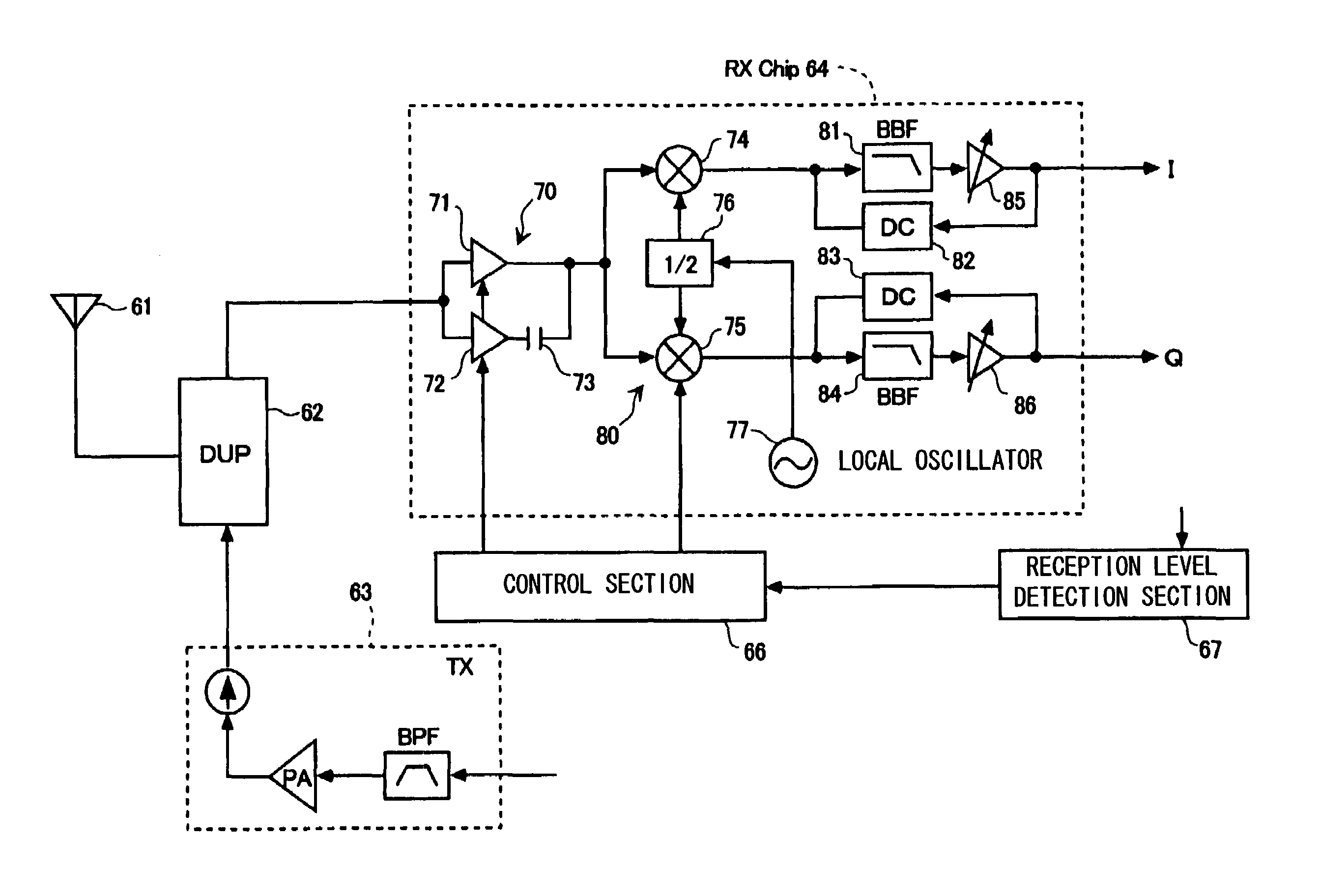
[0028]FIG. 5 shows an example of a configuration of a part of a digital wireless communication terminal containing a direct conversion receiver (DCR) suitable for a wireless communication system using Code Division Multiple Access (CDMA) that relates to the present invention.

[0029]This wireless communication terminal has a transmission circuit 63, a reception circuit 64, an antenna 61, a duplexer 62 for sharing the antenna between transmission and reception, a reception level detection section 67 which detects a reception signal level, and a control section 66 which controls the operation of the reception circuit 64 based on an output from the reception level detection section 67.

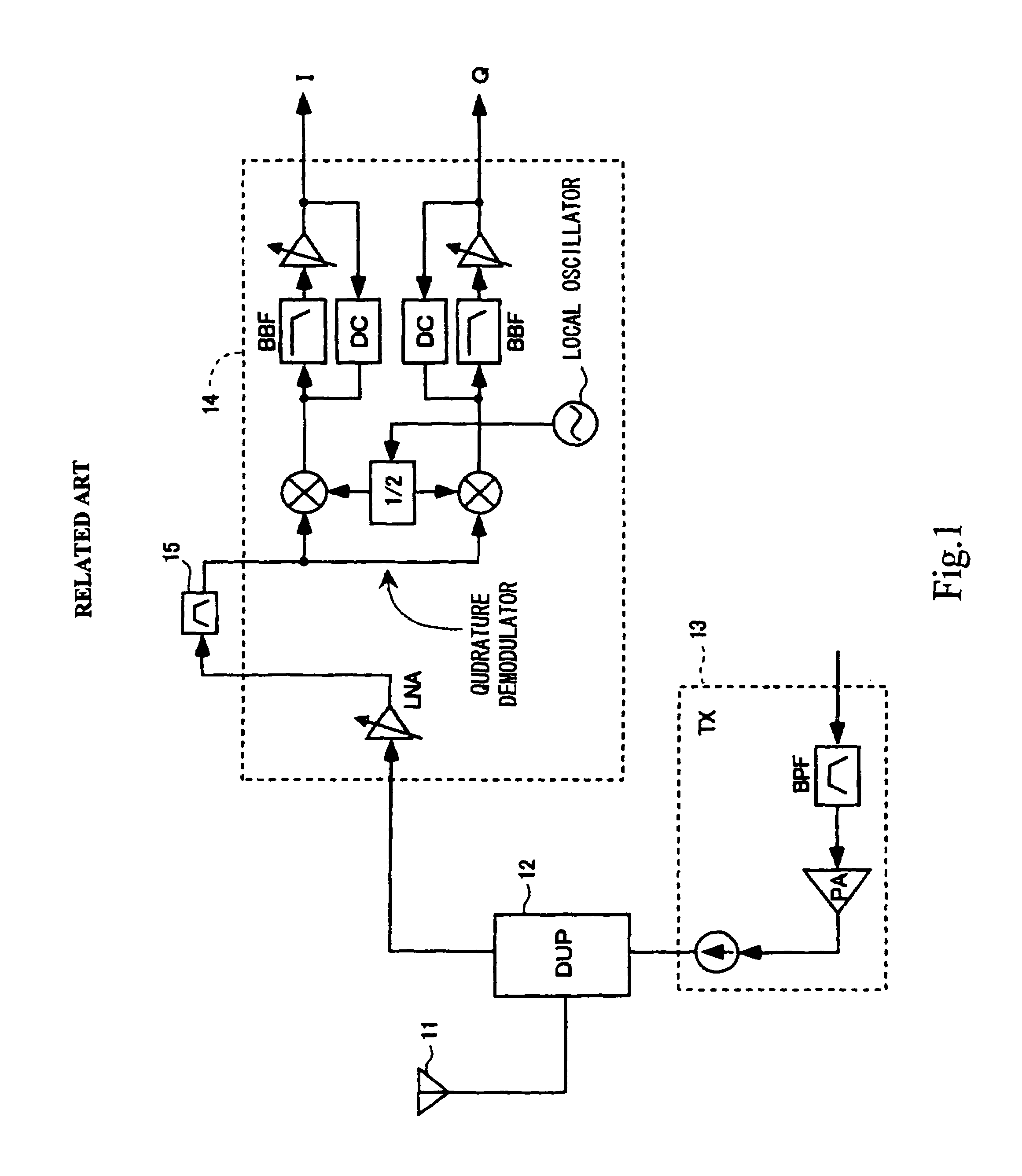
[0030]The reception circuit 64 is formed of an IC chip, and has two LNAs 71 and 72 having different gains, a capacitor 73 connected in series to an output of the LNA 72, a quadrature dem...


PUM


Abstract

There are provided, as a low noise amplifier (70) a low noise amplifier (71) with a low gain and a low noise amplifier (72) with a high gain, selectively operable under control of a bias current, and an output from the low noise amplifier (72) and a quadrature demodulator (80) are connected with a serial capacitance (73) and also an output from the low noise amplifier (71) and the quadrature demodulator (80) are serially connected. A control section (66) controls a reception circuit so that the low noise amplifier (71) operates when a reception signal level is high and the low noise amplifier (72) operates when the reception signal level is low. When the low noise amplifier (72) operates, a DC bias current thereof is made flow separately from a DC bias current of the quadrature demodulator (80), and, when the low noise amplifier (71) operates, a DC bias current thereof is shared with the quadrature demodulator.

Description

TECHNICAL FIELD[0001]The present invention relates to a wireless communication terminal apparatus and its reception circuit, and particularly, to a reception system RF chip for a digital wireless communication terminal.BACKGROUND ART[0002]FIG. 1 shows a configuration of a portion of a wireless communication terminal including a conventional direct conversion receiver (DCR) that relates to the present invention. In this configuration, especially, in a communication system using Code Division Multiple Access (CDMA) represented by a third generation mobile phone (3G), since a reception (RX) signal and a transmission (TX) signal having different frequencies are simultaneously input and output, the local TX signal is leaked to the RX side to degrade reception characteristics. To solve this problem, it is necessary to improve isolation characteristics from a transmission circuit 13 to a reception circuit (RX Chip) 14 in a duplexer (DUP) 12, and it is necessary to insert a band pass filter...

Claims


Application Information

Patent Timeline
Patent Type & Authority Patents(United States)
IPC IPC(8): H04B1/06H03G3/10H04B1/10H04B1/30
CPCH04B1/30H04B1/10H04B1/40
Inventor TAKAGI, KOTARO
Owner SNAPTRACK
Why Eureka
Try Eureka