Flip chip ball grid array package

a grid array and chip ball technology, applied in the field of integrated circuit packaging, can solve the problems of thermally induced stress generation in these packages, poor thermal dissipation performance, and disadvantages of packages, and achieve the effects of reducing stress, effective heat dissipation, and dissipating heat away

Inactive Publication Date: 2007-05-29
UTAC HEADQUARTERS PTE LTD
View PDF15 Cites 64 Cited by
  • Summary
  • Abstract
  • Description
  • Claims
  • Application Information

AI Technical Summary

Benefits of technology

[0012]Advantageously, the use of an intermetallic compound, such as copper aluminide, fixed directly to a silicon wafer provides an effective heat spreader for dissipating heat away from the semiconductor die of the IC package. In one aspect, the intermetalli

Problems solved by technology

Typical BGA packages include a convoluted signal path, giving rise to high impedance and an inefficient thermal path which results in poor thermal dissipation performance.
These packages suffer disadvantages, however.
One particular disadvantage is the generation of thermally induced stress in these packages, due to a mismatch in coefficients of thermal expansion (CTE) between the semiconductor die and t

Method used


Image

  • Flip chip ball grid array package
  • Flip chip ball grid array package
  • Flip chip ball grid array package

Examples


first embodiment

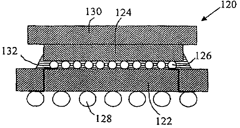
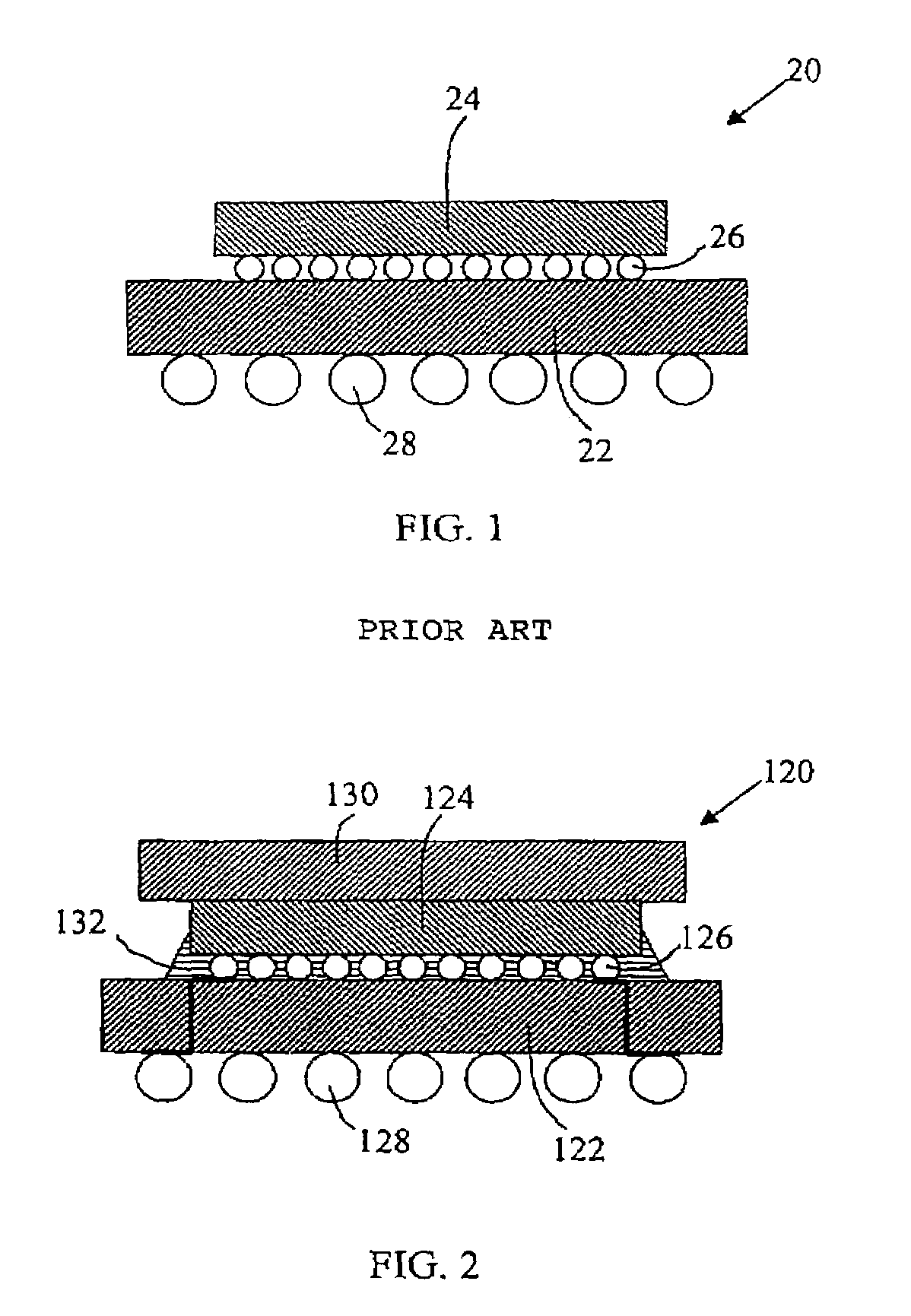
[0018]Reference is now made to FIG. 2 to describe a flip chip ball grid array (BGA) package 20, indicated generally by the numeral 120. To simplify the description, the numerals used previously in describing FIG. 1, will be used again after raising the numerals by 100 where parts to be described correspond to parts already described.

[0019]The flip-chip BGA package 120 includes a substrate 122 having first and second surfaces and a plurality of conductive traces therebetween. A semiconductor die 124 is flip-chip mounted to the first surface of the substrate 122 and electrically connected to ones of the conductive traces. An intermetallic heat spreader 130 is fixed to a backside of the semiconductor die 124 and a plurality of contact balls 128 are disposed on the second surface of the substrate. The contact balls 128 are in the form of a ball grid array and ones of the contact balls 128 of the ball grid array are electrically connected with ones of the conductive traces of the substra...

second embodiment

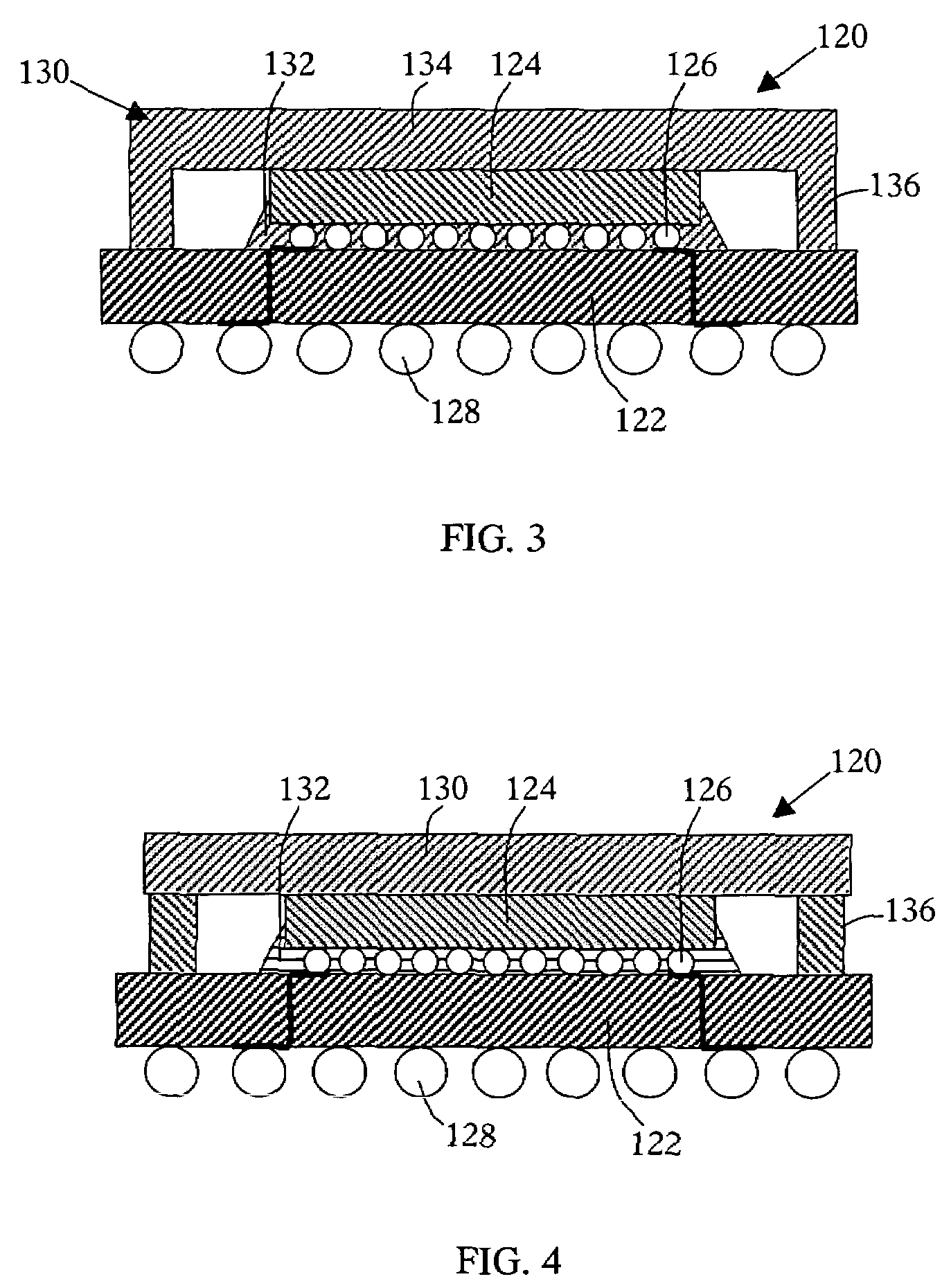
[0026]Reference is now made to FIG. 3 to describe the flip-chip BGA package of the present invention. In this embodiment, the intermetallic heat spreader 130 includes a first flat portion 134 that is fixed to the backside of the semiconductor die 124 and four sidewalls 136 that extend downwardly from the first flat portion, to the substrate 122. Only two of the four sidewalls 136 are shown in the sectional view of FIG. 3. The sidewalls 136 are fixed to the substrate using a thermally conductive adhesive or epoxy, thereby providing additional support and stiffness for the BGA package 120. The remainder of the elements of the present embodiment are similar to those of the first-described embodiment and need not be further described herein.

third embodiment

[0027]Reference is now made to FIG. 4 to describe the flip-chip BGA package of the present invention. In this embodiment, the intermetallic heat spreader 130 is a flat plate that is fixed to the backside of the semiconductor die 124. Four sidewalls 136 are fixed between the intermetallic heat spreader 130 and the substrate 122, at the periphery of the intermetallic heat spreader 130. The sidewalls 136 are fixed to the heat spreader 130 prior to fixing the heat spreader 130 to the semiconductor die 124 and are fixed to the substrate when the heat spreader 130 is fixed to the semiconductor die 124. The sidewalls 136 are fixed to the heat spreader 130 using a thermally conductive epoxy or adhesive, and similarly, the opposing end of the sidewalls 136 are fixed to the substrate using a thermally conductive epoxy or adhesive. The sidewalls 136 can be made of any suitable material including, intermetallic compound, ceramic or metal such as copper, nickel or iron based metals. The sidewall...


PUM


Abstract

A flip-chip ball grid array integrated circuit package with improved thermo-mechanical properties is provided. The package includes a substrate having first and second surfaces and a plurality of conductive traces therebetween. A semiconductor die is flip-chip mounted to the first surface of the substrate and electrically connected to ones of the conductive traces. An intermetallic heat spreader is fixed to a back side of the semiconductor die and a plurality of contact balls are disposed on the second surface of the substrate. The contact balls are in the form of a ball grid array and ones of the contact balls of the ball grid array are electrically connected to ones of the conductive traces.

Description

FIELD OF THE INVENTION[0001]This is a continuation-in-part of U.S. patent application Ser. No. 10 / 211,567 entitled Improved Chip Scale Integrated Circuit Package, filed Aug. 5, 2002, now U.S. Pat. No. 6,667,191.FIELD OF THE INVENTION[0002]The present invention relates in general to integrated circuit packaging, and more particularly to a flip chip ball grid array package with improved thermo-mechanical properties.BACKGROUND OF THE INVENTION[0003]High performance integrated circuit (IC) packages are well known in the art. Improvements in IC packages are driven by industry demands for increased thermal and electrical performance and decreased size and cost of manufacture[0004]In general, array packaging such as Ball Grid Array (BGA) packages provide a high density of interconnects relative to the surface area of the package. Typical BGA packages include a convoluted signal path, giving rise to high impedance and an inefficient thermal path which results in poor thermal dissipation per...

Claims


Application Information

Patent Timeline
IPC IPC(8): H01L23/02H01L23/31H01L23/36H01L23/373
CPCH01L23/3114H01L23/36H01L23/3736H01L2224/16H01L2924/15311H01L2924/3011H01L2924/01322H01L2924/01327H01L2924/00H01L2924/10253H01L2224/05573
Inventor MCLELLAN, NEILYEUNG, TAK SANG
Owner UTAC HEADQUARTERS PTE LTD
Why Eureka
Try Eureka