Supercharge Your Innovation With Domain-Expert AI Agents!

ESD protection circuit for radio frequency input/output terminals in an integrated circuit

a protection circuit and radio frequency input/output terminal technology, applied in the direction of relays, pulse manipulation, pulse techniques, etc., can solve the problems of incomplete failure of the integrated circuit, reduced reliability, and damage to the integrated circuit, and achieve high resistivity and low resistance. , the effect of reducing the risk of damag

Active Publication Date: 2007-05-29
ADVANCED MICRO DEVICES INC
View PDF20 Cites 12 Cited by
  • Summary
  • Abstract
  • Description
  • Claims
  • Application Information

AI Technical Summary

Benefits of technology

[0009]Generally, the present invention is directed at a device and a method that protects an integrated circuit, which is configured to operate in a radio frequency range, from damage by electrostatic discharge events by providing a protection circuit that exhibits a frequency dependent resistance such that radio signals composed of high frequency components are only slightly attenuated, while low-frequency may effectively be shorted to substantially avoid serious over voltage at an internal circuit of the integrated circuit.
[0012]In yet another embodiment a method of reducing the risk of damage caused by an electrostatic discharge event in an integrated circuit having an input terminal and a reference terminal for receiving a radio frequency signal to be provided to an internal circuit is provided. The method comprises providing an ESD protection circuit between the input terminal and the reference terminal such that the ESD protection circuit exhibits a high resistivity at a predefined frequency range including the frequency of the RF signal and providing a low resistivity at frequencies below the specified frequency range.
[0013]In a further embodiment, a method of reducing the risk of damage caused by an electrostatic discharge event in an integrated circuit having an output terminal and a reference terminal for outputting an RF signal supplied by an internal circuit is provided. The method comprises providing an output transistor, one terminal of which is connected to the output terminal. Moreover, an inductive element is provided, one end of which is coupled to the output terminal, the other end of which is coupled to an auxiliary voltage node. The method further includes providing first and second clamping elements between the auxiliary voltage node and high supply voltage line and the auxiliary voltage node and a low supplied voltage line, respectively, so that upon occurrence of an over voltage at the output terminal, the output terminal is clamped to the high supply voltage line and the low supply voltage line, respectively, via the inductive element and one of the first and second clamping elements.

Problems solved by technology

Any over voltage supplied to a thin gate insulation layer, however, will lead to defects in the gate insulation layer, resulting in a reduced reliability, or may even completely destroy the elements, possibly resulting in a complete failure of the integrated circuit.
For example, a person can develop very high static voltage from a few hundred to several thousand volts, merely by moving across a carpet, so that an integrated circuit may be damaged when the person contacts the integrated circuit, for example, by removing the integrated circuit from the corresponding circuit board.
A corresponding over voltage caused by an ESD event may even occur during the manufacturing of the integrated circuit and may thus lead to a reduced product yield.
For example, in modern wireless communications systems, commonly integrated circuits including a large number of MOS transistors are used that are intended to operate up to several GHz (gigahertz) and hence, adequate protection of the corresponding terminals receiving or outputting any signals in this frequency range may not adequately be protected against ESD events, since the associated parasitic capacitances do not allow to form sufficiently sized protective elements without unduly degrading the performance of the integrated circuit.

Method used


Image

  • ESD protection circuit for radio frequency input/output terminals in an integrated circuit
  • ESD protection circuit for radio frequency input/output terminals in an integrated circuit
  • ESD protection circuit for radio frequency input/output terminals in an integrated circuit

Examples


Embodiment Construction

[0020]It is to be noted that although the present invention is described with reference to the embodiments as illustrated in the following detailed description and in the accompanying drawings, the detailed description, as well as the drawings, are not intended to limit the present invention to the particular embodiments disclosed therein, but rather, the described embodiments merely exemplify the various aspects of the present invention, the scope of which is defined by the appended claims.

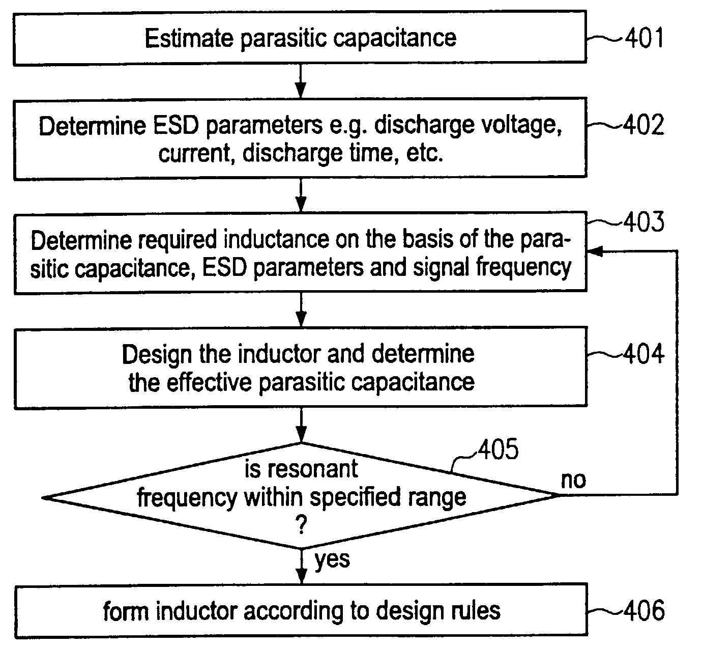
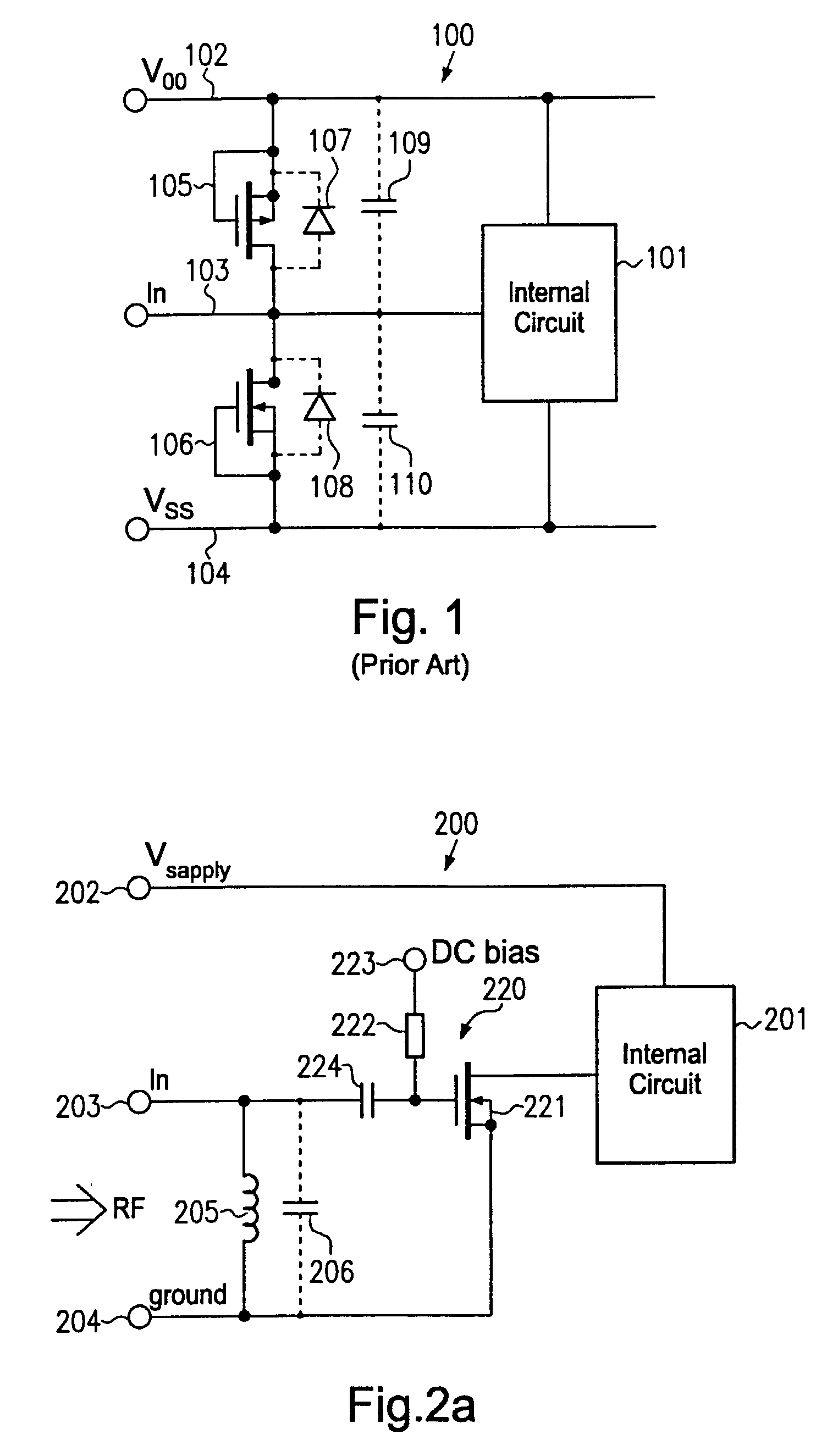
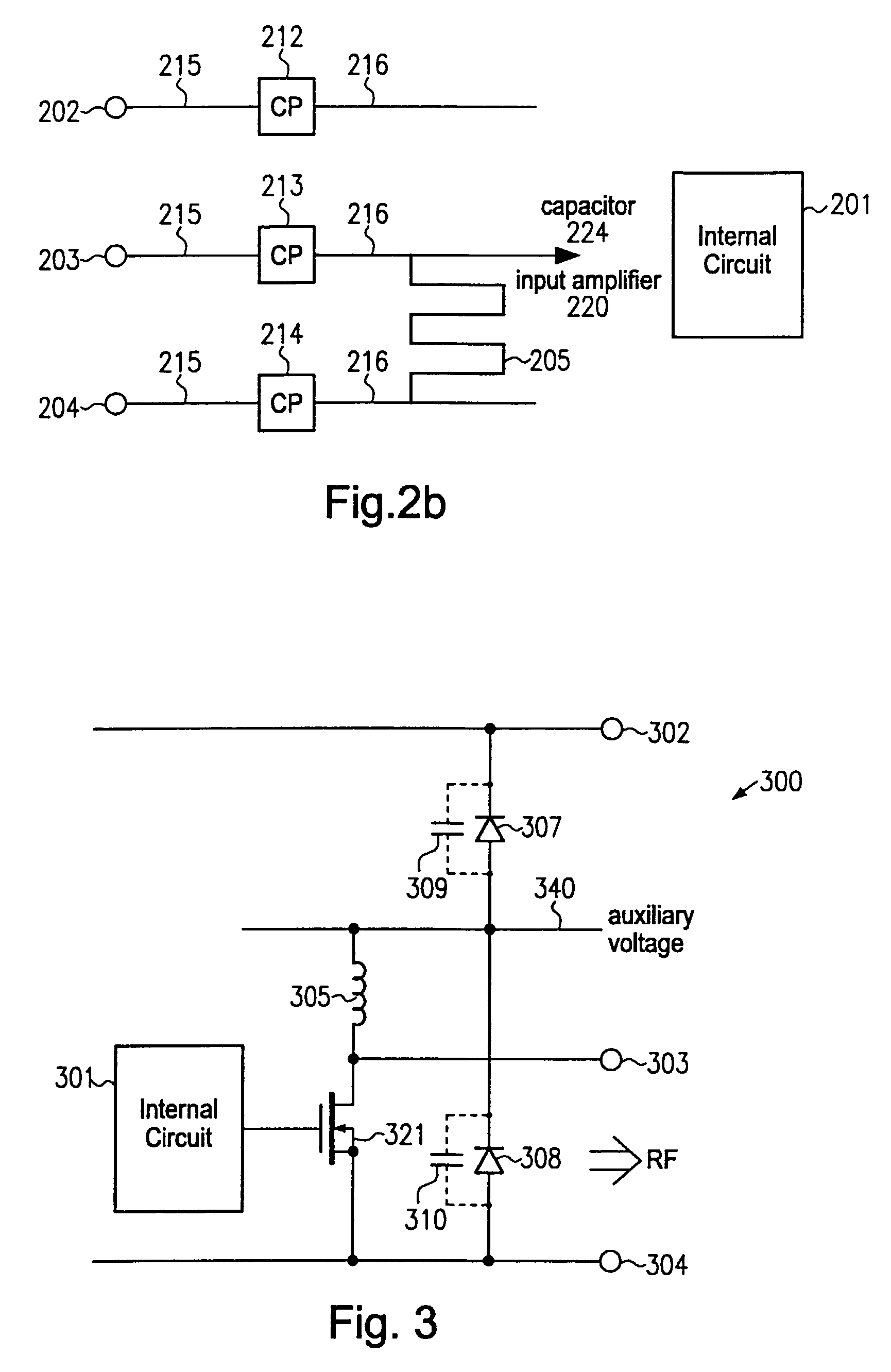
[0021]With reference to FIGS. 2 to 4, illustrative embodiments will now be described, which are directed at the problem of reducing the risk of damage caused by any electrostatic discharge events occurring on input and / or output terminals of integrated circuits. Also, in the following detailed description, reference will be made to ESD events involving a voltage of the order of 2000-3000 volts at a rise time of about 100 ns, with a discharge current of several amperes. These parameters correspond...


PUM


Abstract

An integrated circuit comprises an ESD protection circuit including an inductor coupled between an input terminal and a ground terminal at which an RF signal is applied. The inductor is designed so as to provide a sufficient current capability required in typical ESD events. Moreover, the inductance of the inductor is selected to define, in combination with any parasitic capacitance present, a resonance tank with a resonant frequency that is matched to the RF signal. Accordingly, the operating frequency of the integrated circuit is not limited by the ESD protection circuit. In a further embodiment, an output terminal is ESD protected by an inductor that is coupled to an auxiliary voltage serving to bias an output transistor. Moreover, clamping elements, such as diodes, are provided between the auxiliary voltage and the supply voltage and between the auxiliary voltage and ground potential.

Description

FIELD OF THE NEW INVENTION[0001]The present invention generally relates to the field of integrated circuits having an internal circuitry for receiving and / or outputting radio frequency signals, wherein a protection circuit is provided to minimise the risk of damage due to electrostatic discharge (ESD) events.DESCRIPTION OF THE RELATED ART[0002]In modern integrated circuits usually a huge number of individual circuit elements, such as field effect transistors, capacitors, resistors and the like are formed on a small substrate area so as to provide for the required functionality of the circuitry. Typically, a number of contact pads are provided, which in turn, are electrically connected to respective terminals, also referred to as pins, to allow the circuitry to communicate with the environment. As feature sizes of the circuit elements are steadily shrinking to increase package density and enhance the performance of the integrated circuit, the ability for withstanding an externally ap...

Claims


Application Information

Patent Timeline
IPC IPC(8): H04B1/16H01L27/02
CPCH01L27/0251H01L2924/0002H01L2924/00
Inventor KLUGE, WOLFRAMHUSCHKA, ANDREASHAHN, UWE
Owner ADVANCED MICRO DEVICES INC
Features
  • R&D
  • Intellectual Property
  • Life Sciences
  • Materials
  • Tech Scout
  • Unparalleled Data Quality
  • Higher Quality Content
  • 60% Fewer Hallucinations
Learn More