Structure and method for enhanced performance in semiconductor substrates

a technology of semiconductor substrates and structures, applied in the direction of semiconductor devices, basic electric elements, electrical apparatus, etc., can solve the problem of limiting the thickness reduction that may be applied to the substrate, and achieve the effect of facilitating die separation and improving electrical and thermal performan

Inactive Publication Date: 2007-06-05
POWER INTEGRATIONS INC
View PDF2 Cites 20 Cited by
  • Summary
  • Abstract
  • Description
  • Claims
  • Application Information

AI Technical Summary

Benefits of technology

[0009]Accordingly, embodiments of the present invention are directed toward an etched substrate structure that may augmented by conductive material to provide enhanced electrical and thermal performance, or aligned with die separation lines to facilitate die separation.

Problems solved by technology

However, wafer handling considerations and electrical requirements limit the reduction in thickness that may be applied to the substrate 105 and epitaxial layer 115.
Thus, in conventional semiconductor substrates there is frequently a bulk region that either contributes to undesirable resistance in operational electrical or thermal paths, or provides an additional current path with undesirable properties.

Method used


Image

  • Structure and method for enhanced performance in semiconductor substrates
  • Structure and method for enhanced performance in semiconductor substrates
  • Structure and method for enhanced performance in semiconductor substrates

Examples


Embodiment Construction

[0021]In the following detailed description of the present invention, a structure and method for enhanced performance in semiconductor substrates, numerous specific details are set forth in order to provide a thorough understanding of the present invention. However, it will be obvious to one skilled in the art that the present invention may be practiced without these specific details. In other instances well known circuits and components have not been described in detail so as not to unnecessarily obscure aspects of the present invention.

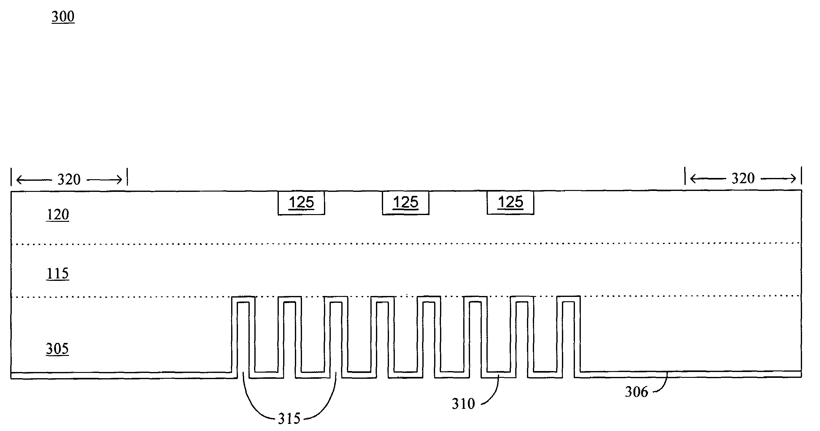
[0022]FIG. 3A shows a semiconductor device 300 in accordance with an embodiment of the present invention. The active regions 125, epitaxial layers 115 and 120 are similar to those shown in FIG. 1. However, the substrate 305 has a number of blind features 315 that are coated with a conductive layer 310.

[0023]In one embodiment, the blind features 315 are created by etching of the bottom surface 306 of the substrate 305 through a mask. The blind featur...


PUM

PropertyMeasurementUnit
areaaaaaaaaaaa
electrical conductivityaaaaaaaaaa
thermal conductivityaaaaaaaaaa

Abstract

An etched substrate structure is augmented by conductive material to provide enhanced electrical and/or thermal performance. A semiconductor device substrate comprising active regions defined on a top surface is masked and etched to define a pattern of blind features in a bottom surface of the substrate. A conductive material is then deposited on the surface of the blind features. The replacement of semiconductor material with the conductive material lowers the resistance between the active elements on the top surface and the bottom surface. The blind features may be placed in proximity to parasitic bipolar transistors in order to increase immunity to latchup. During wafer processing, a pattern of grooves aligned opposite to a scribe street pattern may be etched on the wafer back side in order to facilitate the separation of individual devices.

Description

FIELD OF THE INVENTION[0001]Embodiments of the present invention relate to the field of semiconductor devices. In particular, embodiments of the present invention relate to the electrical and thermal resistances of semiconductor device substrates.BACKGROUND ART[0002]Prior Art FIG. 1 shows a general example of a semiconductor device 100. The semiconductor device 100 has a substrate 105 with a back side metal layer 110, a first epitaxial layer 115, and a second epitaxial layer 120. A number of active regions 125 are disposed in the second epitaxial region 120. The active regions 125 contain circuit elements such as transistors or diodes that conduct electric current and dissipate heat. Examples of transistors are bipolar junction transistors (BJTs), metal-oxide field effect transistors (MOSFETs), and junction field effect transistors (JFETs).[0003]The back side metal layer is commonly used to provide an electrical contact (e.g., ground) to the substrate 105 and to provide a solderable...

Claims


Application Information

Patent Timeline
Patent Type & Authority Patents(United States)
IPC IPC(8): H01L29/06
CPCH01L27/0921H01L29/0661H01L29/78H01L2924/10158
Inventor LIN, CHONG MINGDENNING, JAYYU, HO YUAN
Owner POWER INTEGRATIONS INC
Why Eureka
Try Eureka