Circuit and method for compensating for offset voltage

a technology of offset voltage and circuit, applied in pulse manipulation, pulse technique, instruments, etc., can solve the problems of low transmission rate, low storage capacity, and inability to provide a direct solution to the problem caused

Inactive Publication Date: 2007-06-05
SAMSUNG ELECTRO MECHANICS CO LTD
View PDF5 Cites 55 Cited by
  • Summary
  • Abstract
  • Description
  • Claims
  • Application Information

AI Technical Summary

Benefits of technology

[0028]Accordingly, the present invention has been made keeping in mind the above problems occurring in the prior art, and an object of the present invention is to provide a compensation circuit, which is capable of compensating for the characteristics of BJTs depending on variation in surrounding temperature in a circuit including the BJTs.
[0029]Another object of the present invention is to provide a circuit, which is capable of compensating for variation in characteristics of BJTs depending on temperature.
[0030]A further object of the present invention is to provide a method of compensating for the operational characteristics of the circuit depending on variation in temperature.

Problems solved by technology

However, the optical storage technology is disadvantageous in that its transmission rate is low and its storage capacity is low.
Although the disclosed scheme may be a next best measure for compensating for operational variation depending on variation in temperature, it does not provide a direct solution to the problem caused by variation in the operational value of elements depending on variation in temperature.

Method used


Image

  • Circuit and method for compensating for offset voltage
  • Circuit and method for compensating for offset voltage
  • Circuit and method for compensating for offset voltage

Examples


Embodiment Construction

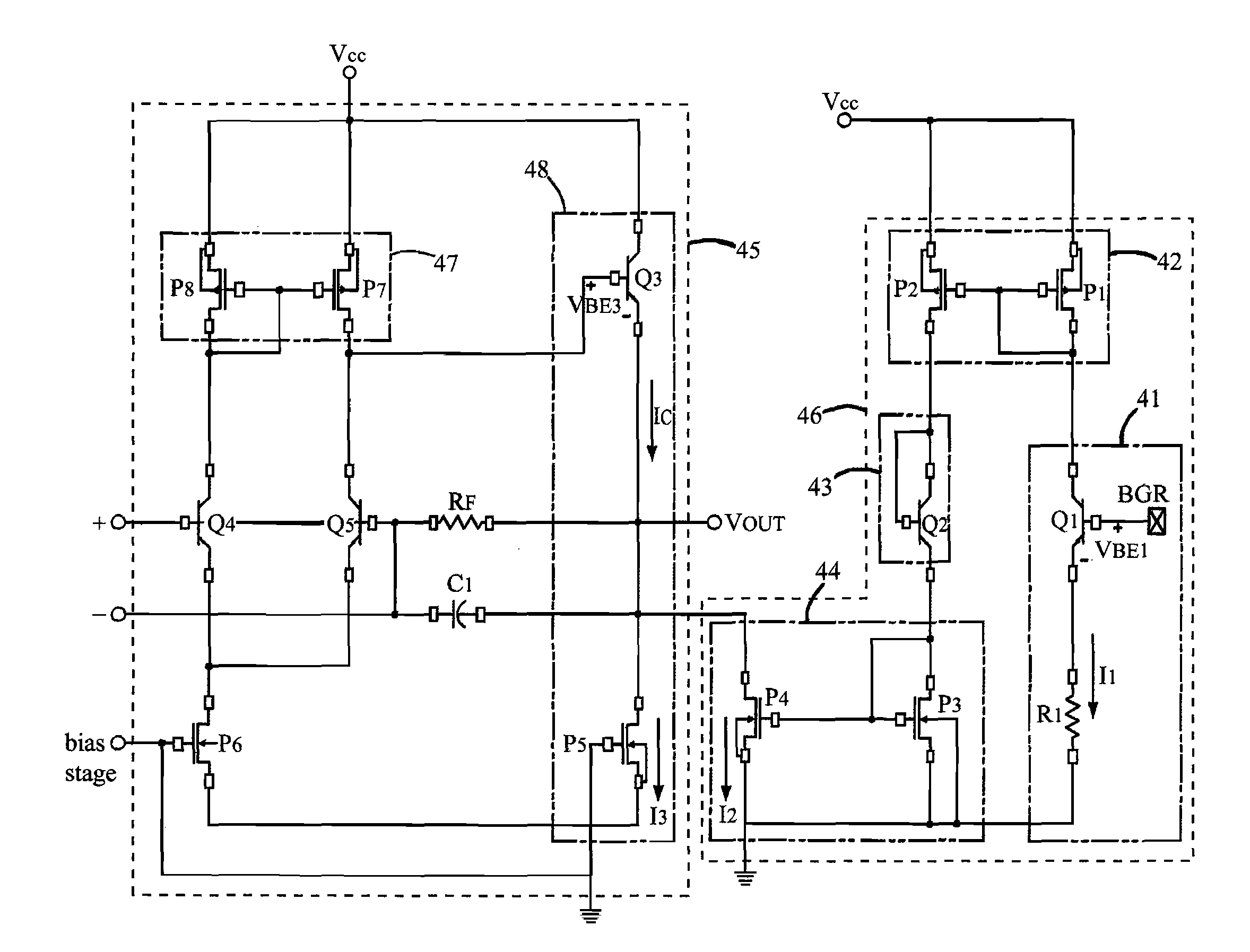
[0042]Embodiments of the present invention are described in detail with reference to the accompanying drawings below.

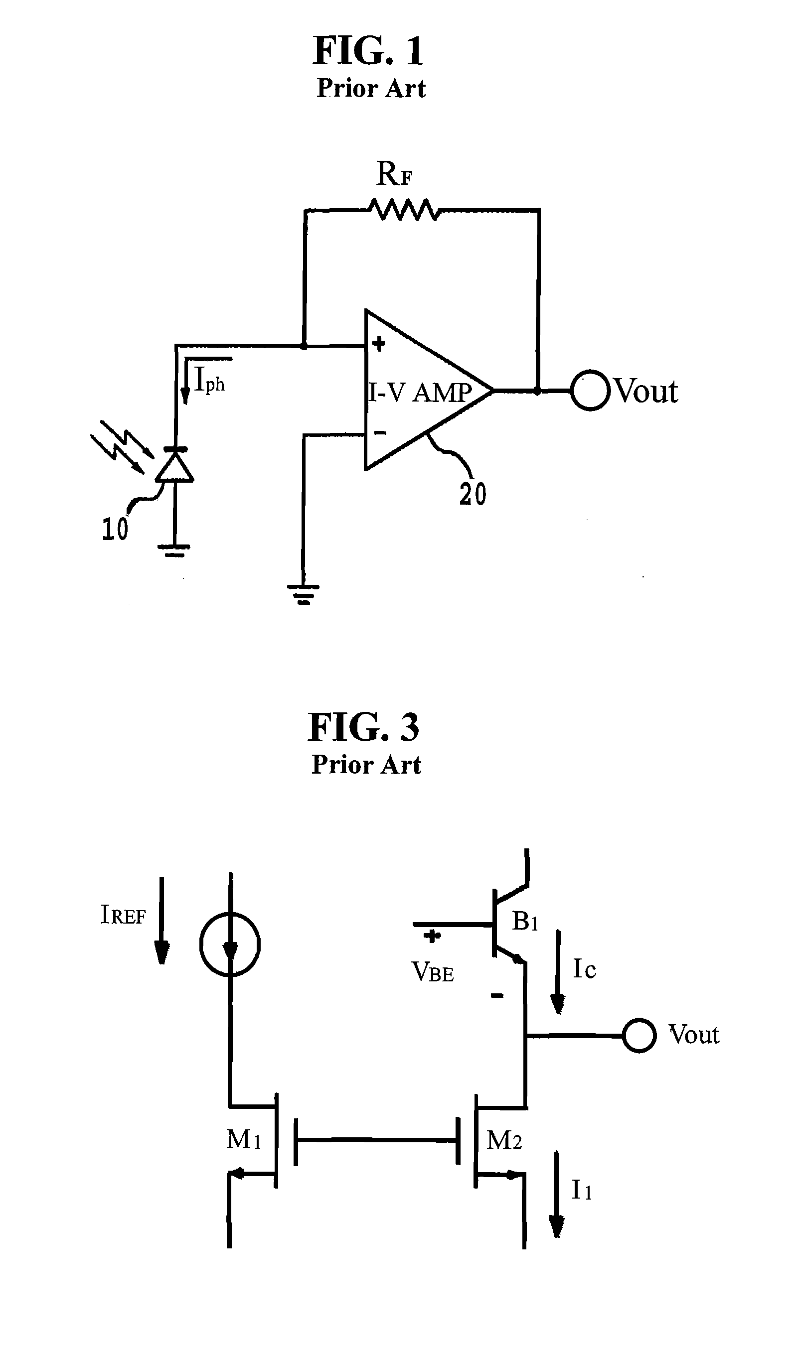
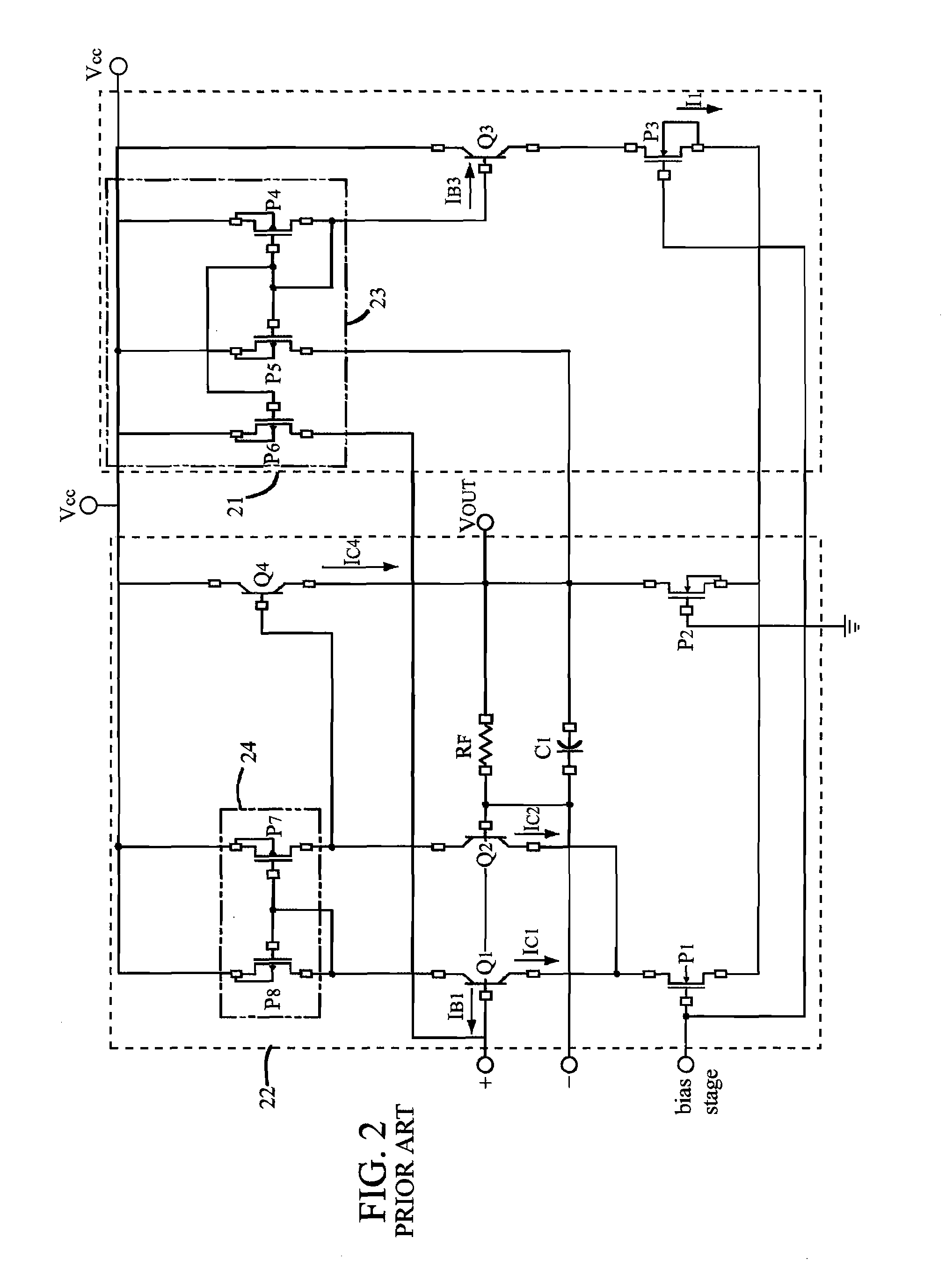
[0043]FIG. 3 is a circuit diagram illustrating the variation in output voltage depending on variation in surrounding temperature, which shows the construction of the output stage of a typical current-voltage conversion amplifier. When temperature increases, the base-emitter voltage VBE of a transistor B1, which is a BJT, decreases by 2 mV per 1° C. In this case, an output voltage VOUT decreases because a current Ic is fixed at the same magnitude as a current I1.

[0044]In this case, the current Ic, which flows through the transistor B1, and the base-emitter voltage VBE have a relationship as in the following Equation 1:

[0045]Ic=Is⁢ⅇVBEVT(1)

where Is is the intrinsic saturation current value of the BJT B1, and VT is a intrinsic threshold voltage value of the BJT B1, which has a constant value.

[0046]Accordingly, based on the above-described relationship, with respect to th...


PUM


Abstract

A circuit for compensating for an offset voltage in a PhotoDetector Integrated Circuit (PDIC). The circuit includes a temperature detection unit, a current transfer unit and a current adjustment unit. The temperature detection unit generates a current that varies with variation in surrounding temperature. The current transfer unit transfers the generated current. The current adjustment unit adjusts the current transferred from the current transfer unit at a predetermined ratio and outputs the adjusted current.

Description

INCORPORATION BY REFERENCE[0001]The present application claims priority under 35 U.S.C. §119 to Korean Patent Application No. 2005-15020 filed on Feb. 23, 2005. The content of the application is incorporated herein by reference in its entirety.BACKGROUND OF THE INVENTION[0002]1. Field of the Invention[0003]The present invention relates generally to a circuit and method for compensating for variation in an offset voltage depending on variation in temperature in a photodiode integrated circuit and, more particularly, to a circuit and method capable of compensating for variation in an offset voltage depending on variation in surrounding temperature by adding a circuit for varying currents flowing through bipolar junction transistors, the characteristics of which varies with variation in surrounding temperature, according to variation in temperature.[0004]2. Description of the Related Art[0005]Recently, optical storage technology is developing toward high density, high speed and compact...

Claims


Application Information

Patent Timeline
Patent Type & Authority Patents(United States)
IPC IPC(8): H03K5/22
CPCH03F3/087H03F3/45291H03F3/45748H03F3/45896H03F3/45973H03F2200/447G11B7/13G11B20/10
Inventor GONG, JUNG CHULKWON, KYOUNG SOOHWANG, HYEON SEOKKIM, SANG SUK
Owner SAMSUNG ELECTRO MECHANICS CO LTD
Why Eureka
Try Eureka