Semiconductor device having transferred integrated circuit

a technology of integrated circuit and semiconductor, which is applied in the direction of semiconductor devices, solid-state devices, basic electric elements, etc., can solve the problems of disadvantage and high cost of the semiconductor process, and achieve the effects of reducing mounting area, reducing cost, and saving weigh

Inactive Publication Date: 2007-06-12
SEMICON ENERGY LAB CO LTD
View PDF26 Cites 196 Cited by
  • Summary
  • Abstract
  • Description
  • Claims
  • Application Information

AI Technical Summary

Benefits of technology

[0042]According to the present invention, further weight saving, thinning, lower cost, mounting area reduction can be realized, and various complex circuits can be integrated.INDUSTRIAL APPLICABILITY
[0043]According to the present invention, a part or all parts of an electronic device can be manufactured by an assembly to which a plastic sheet provided with various functional circuits or elements is connected, and further lightweight of an information terminal device is realized

Problems solved by technology

Because a semiconductor process generally has a high cost, however, when a large area is needed for a passive element, the cost is disadvantageous.

Method used


Image

  • Semiconductor device having transferred integrated circuit
  • Semiconductor device having transferred integrated circuit
  • Semiconductor device having transferred integrated circuit

Examples


embodiment mode 1

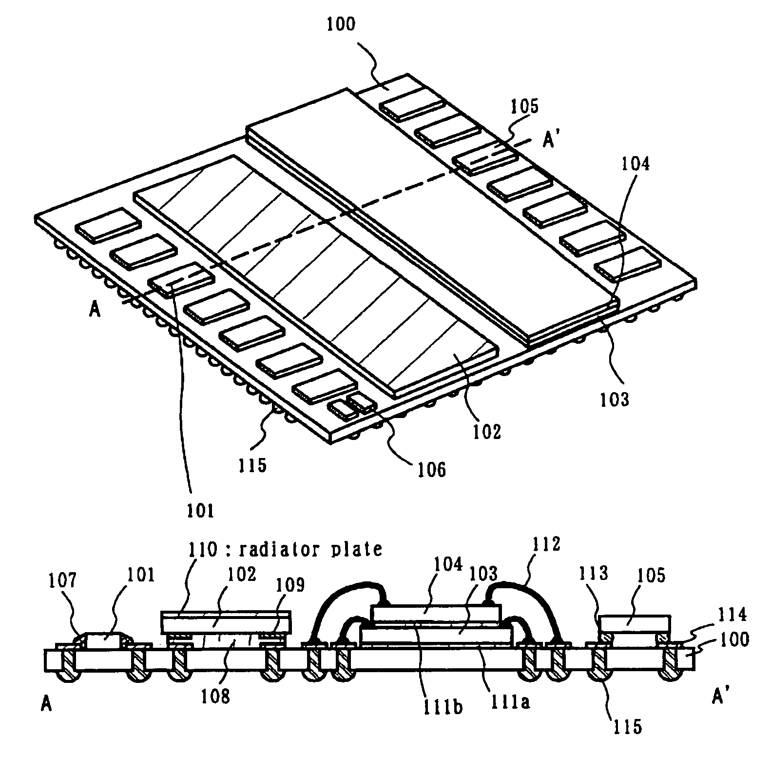
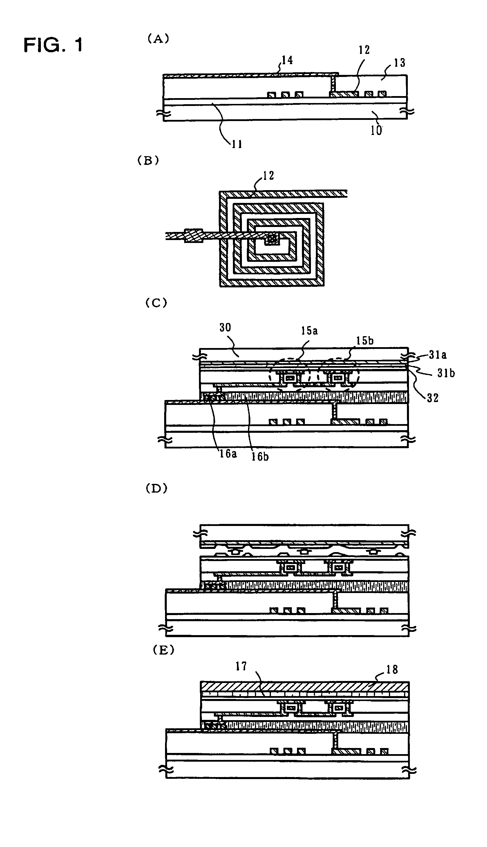
[0058]An example is shown here, in which a laminated capacitor or a laminated inductor is formed without using a semiconductor substrate, transferred to and mounted on a circuit board (printed board).

[0059]First, a heat-resisting glass substrate (e.g. a quartz substrate) or a ceramics substrate is prepared.

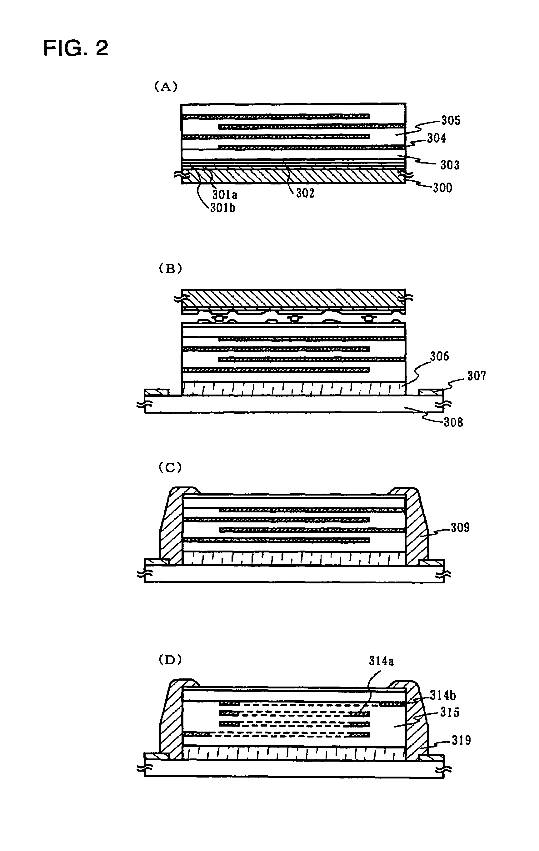
[0060]An example which a laminated capacitor is formed on a substrate (a first substrate 300) is described with reference to FIGS. 2(A) to 2(C). A ceramic substrate is employed in this embodiment since baking at a high temperature is performed. A metal film 301a, here, a tungsten film (from 10 nm to 200 nm in the film thickness, preferably, from 50 nm to 75 nm) is formed by a sputtering method on this ceramic substrate, and further, an oxide film 302, here a silicon oxide film (from 150 nm to 200 nm in the film thickness) is laminated without being exposed to the air. The film thickness of the oxide film 302 is preferably equal to or more than twice the film thickness of the metal...

embodiment mode 2

[0079]An example in which a capacitor element and a TFT are formed, transferred to and mounted on a circuit board (printed board) is shown here.

[0080]Note that the same reference numerals are used for the same portions, since up to a halfway step is performed similarly to Embodiment Mode 1.

[0081]A tungsten film 301a and a silicon oxide film 302 are laminated by a sputtering method over a first substrate 300, and a tungsten oxide film in an amorphous state is formed in forming the silicon oxide film. A silicon oxynitride film (100 nm in film thickness) (not shown in the figure) to be a base insulating film is formed by a PCVD method, and further an amorphous silicon film including hydrogen (55 nm in film thickness) is laminated as a hydrogen containing film without being exposed to the air. Herein, a quartz substrate is used as the first substrate 300.

[0082]A hydrogen concentration of the amorphous silicon film including hydrogen was measured through FT-IR. As a result, Si—H was 1.06...

embodiment mode 3

[0107]An example of a mounting method that is different from that shown in Embodiment Mode 2 is shown in FIG. 4 herein.

[0108]Here, a CMOS circuit in which a p-channel TFT 303a and an n-channel TFT 303b are complementarily combined is formed.

[0109]First, the p-channel TFT 303a and the n-channel TFT 303b are formed on a first substrate according to Embodiment Mode 2 (FIG. 4(A)). Since it is possible that the process temperature in forming a CMOS circuit is controlled to be equal to or less than 600° C., a glass substrate can be used in this embodiment mode for the first substrate 300.

[0110]When a state of FIG. 4(A) is obtained, a circuit board 510 provided with a terminal 509 is bonded to the first substrate 300 by an adhesive agent 508b containing electrical conductive particles 508a (FIG. 4(B)). The terminal 509 and an extraction electrode connected to a TFT are electrically connected via the electrical conductive particles by bonding them.

[0111]Then, the first substrate 300 is sepa...


PUM


Abstract

It is an object to provide a semiconductor device integrating various elements without using a semiconductor substrate, and a method of manufacturing the same. According to the present invention, a layer to be separated including an inductor, a capacitor, a resistor element, a TFT element, an embedded wiring and the like, is formed over a substrate, separated from the substrate, and transferred onto a circuit board 100. An electrical conduction with a wiring pattern 114 provided in the circuit board 100 is made by a wire 112 or a solder 107, thereby forming a high frequency module or the like.

Description

BACKGROUND OF THE INVENTION[0001]1. Field of the Invention[0002]The present invention relates to a TFT, a resistor element, an LC element attenuating a predetermined frequency band, a semiconductor device on which an integrated circuit combining these elements is mounted, and a method of manufacturing the same.[0003]Note that a semiconductor device in this specification means general devices which can function by using semiconductor characteristics, and all of electro-optic devices, semiconductor circuits and electronic devices are the semiconductor devices.[0004]2. Description of the Related Art[0005]A high frequency integrated circuit (also referred to as MMIC) in which an active element such as a transistor and a passive element such as a capacitor, a resistor or an inductor are formed on one semiconductor substrate is known. An active element such as a MESFET, a HEMT, or a HBT, and a lumped parameter element such as a capacitor, an inductor, or a resistor, and a distributed para...

Claims


Application Information

Patent Timeline
Patent Type & Authority Patents(United States)
IPC IPC(8): H01L29/00H01L23/48H01L23/52H01L27/108H01L29/04H01L21/336H01L21/60H01L21/68H01L23/538H01L27/06H01L27/12H03H3/08
CPCH01L21/6835H01L23/5385H01L23/5388H01L24/81H01L27/0688H01L27/12H03H3/08H01L29/66757H01L2221/68354H01L2221/68359H01L2221/68363H01L2221/68368H01L2224/16145H01L2224/32145H01L2224/48091H01L2224/81801H01L2924/01012H01L2924/01013H01L2924/01025H01L2924/01029H01L2924/0103H01L2924/01046H01L2924/01056H01L2924/0106H01L2924/01073H01L2924/01077H01L2924/01078H01L2924/01079H01L2924/01082H01L2924/14H01L2924/1423H01L2924/15311H01L2924/19041H01L2924/19042H01L2924/19043H01L2924/3011H01L2224/16225H01L2224/32225H01L2224/48227H01L2224/73265H01L2924/13063H01L24/48H01L2924/01005H01L2924/01006H01L2924/01023H01L2924/01024H01L2924/01033H01L2924/01041H01L2924/01042H01L2924/01045H01L2924/01047H01L2924/0105H01L2924/01055H01L2924/01074H01L2924/01087H01L2924/014H01L2224/92247H01L2924/19105H01L2224/73204H01L2924/10253H01L2924/13064H01L2924/00014H01L2924/00H01L2924/00012H01L2924/15787H01L2924/15788H01L2924/181H01L2924/12034H01L2924/12042H01L24/73H01L2224/45099H01L2224/45015H01L2924/207
Inventor YAMAZAKI, SHUNPEITAKAYAMA, TORUMARUYAMA, JUNYAOHNO, YUMIKOGOTO, YUUGOKUWABARA, HIDEAKI
Owner SEMICON ENERGY LAB CO LTD
Why Eureka
Try Eureka