Logic circuits utilizing gated diode sensing

a logic circuit and diode sensing technology, applied in the field of logic circuits, can solve the problems of significant reduction of switching power, inability of logic circuits based on traditional field-effect transistor designs to accurately sense and perform logic operations on small logic signals, and inability to handle small logic signals. , to achieve the effect of low vt variation

Inactive Publication Date: 2007-06-12
GOOGLE LLC
View PDF2 Cites 11 Cited by
  • Summary
  • Abstract
  • Description
  • Claims
  • Application Information

AI Technical Summary

Benefits of technology

[0007]The disclosed gated diode logic circuits overcome the Vt variation problem in FETs by detecting and amplifying the small logic signals utilizing gated diodes that have very low Vt variation. The amplified signals may then be processed by conventional logic circuits. The Vt variation of the gated diode is relatively small compared to the small logic signal amplitude and can be controlled relatively precisely. Typically, Vt of the gated diode can be set to half that of the small logic signal amplitude. Thus, the gated diode circuit can sense and amplify the small logic signals sufficiently to perform the various logic operations in conjunction with conventional logic circuits. The output of the logic circuit can be of a standard full CMOS voltage swing, or can be scaled down in amplitude.

Problems solved by technology

Small amplitude signals which can significantly reduce switching power, however, require small signal detection and amplification at the receiving end to differentiate logic levels.
Logic circuits based on traditional Field-Effect Transistor designs are therefore not able to accurately sense and perform logic operations on small logic signals.
This is true for both current and future generations of integrated circuit technologies and, thus, conventional FET logic circuits are not able to handle small logic signals.
For example, when voltages under one volt are being used as the high logic level for small amplitude signals, traditional logic circuits are often unable to reliably detect the signal's high logic level without the use of small signal sensing circuits.
Single ended sense amplifiers for small signals remain a challenge as the reference voltage point used to separate the 0- and 1-state of the small signal may vary as much as the small signal itself, due to variations in the manufacturing process, device threshold voltage, and temperature.

Method used


Image

  • Logic circuits utilizing gated diode sensing
  • Logic circuits utilizing gated diode sensing
  • Logic circuits utilizing gated diode sensing

Examples


Embodiment Construction

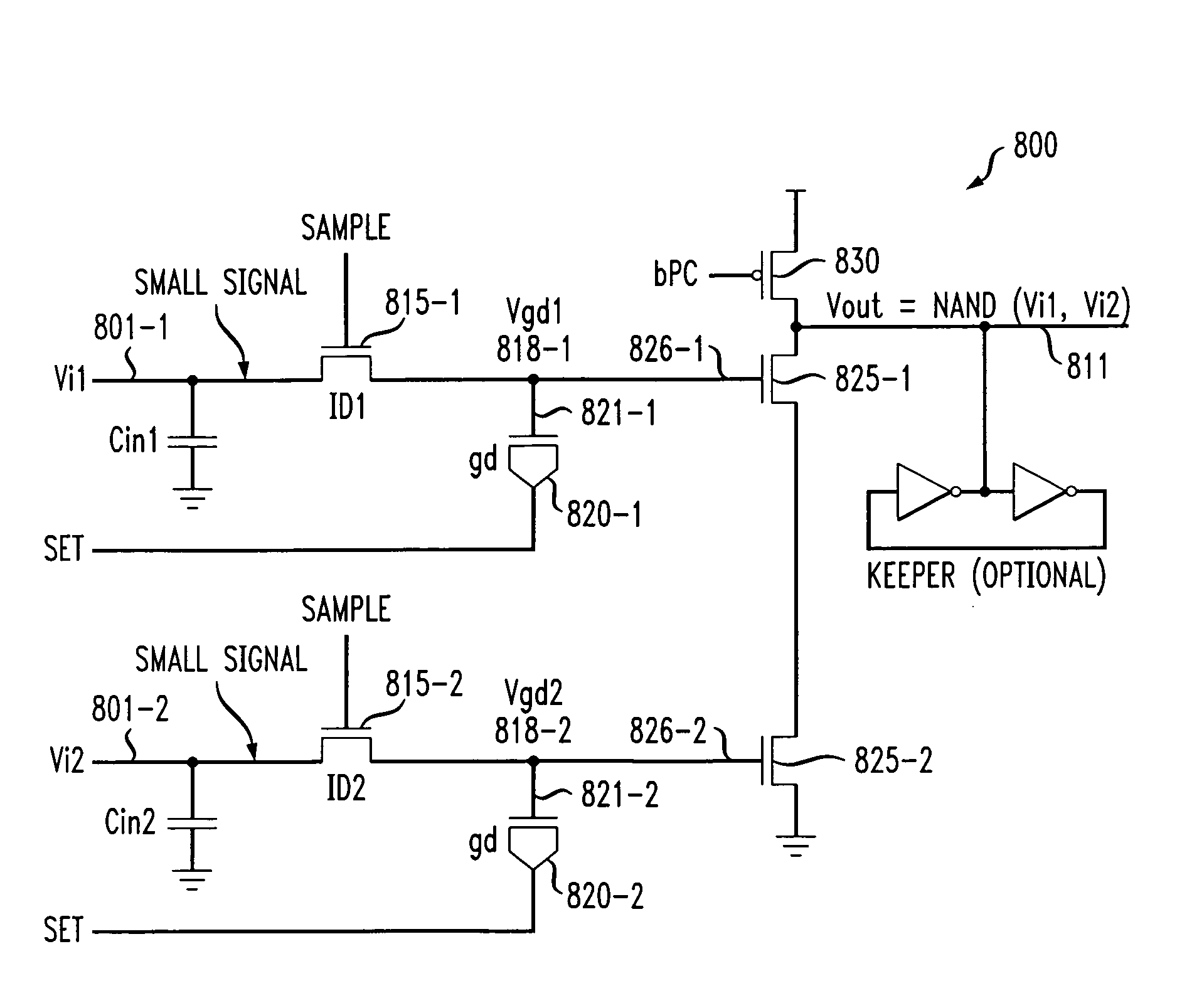
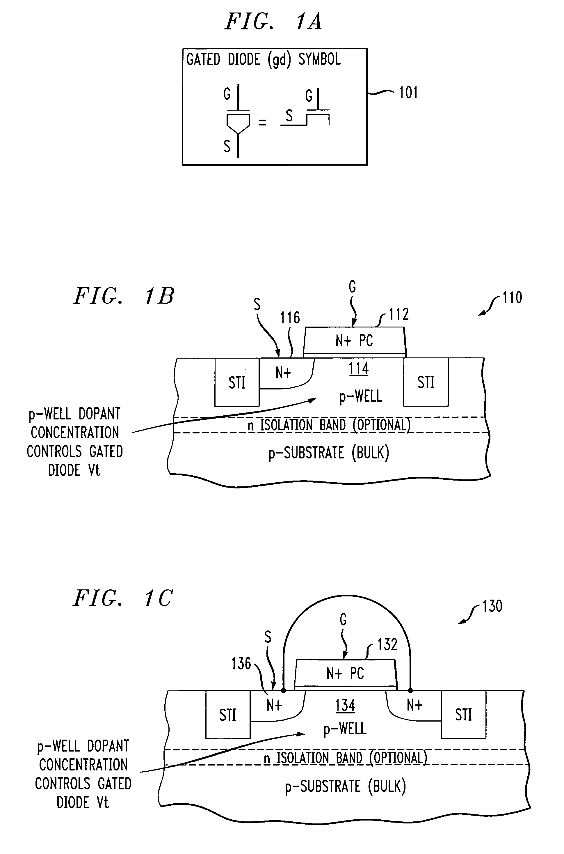
[0039]U.S. patent application Ser. No. 10 / 751,714, entitled “Amplifiers Using Gated Diodes,” incorporated by reference herein, describes an exemplary amplifier circuit for signal amplification and single ended small signal sensing based on gated diode circuitry. The gated diode amplifiers have the unique characteristic of providing high gain and high signal margin, and are tolerant of supply voltage, threshold voltage and process variation. Details about the gated diode characteristic, the principle of operation of the gated diode and the gated diode amplifier are described in the above-identified patent application.

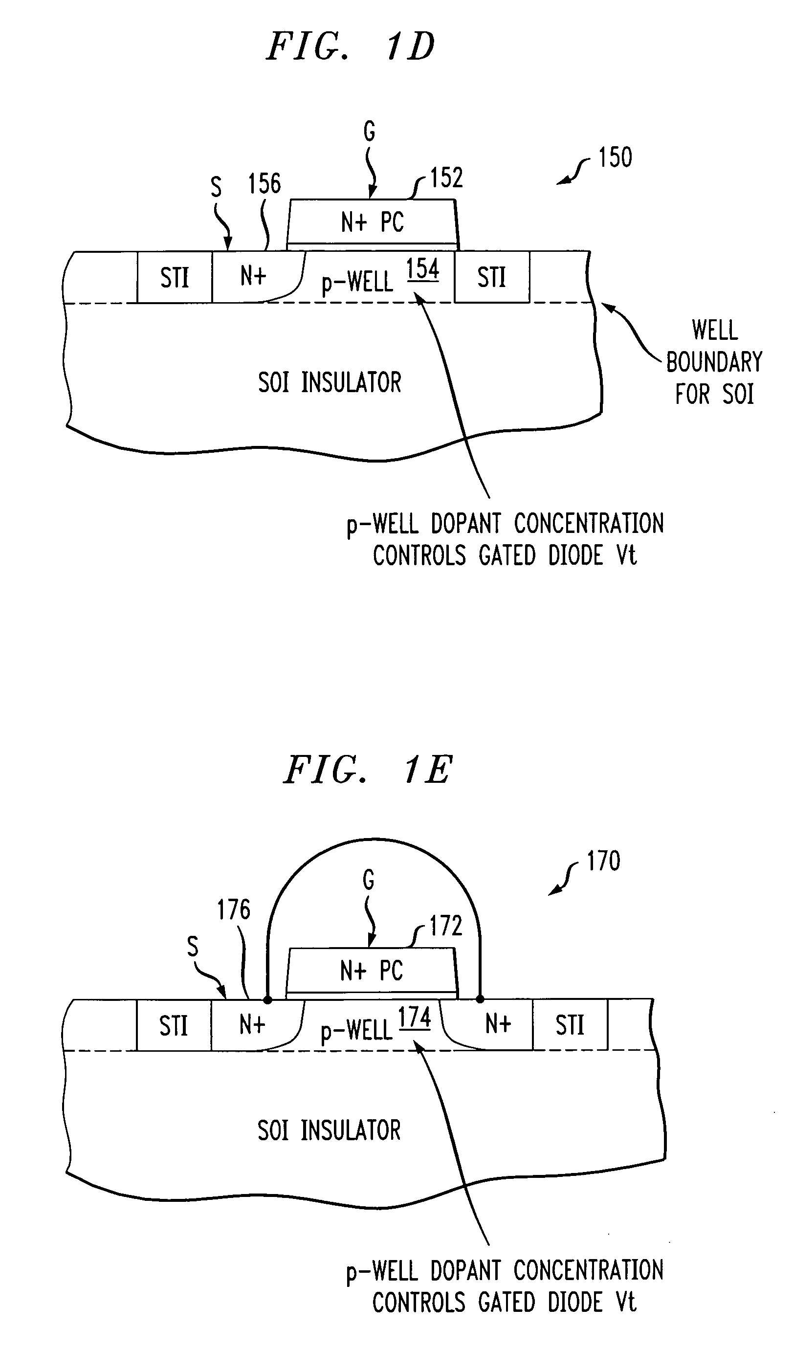
[0040]FIG. 1A shows equivalent symbols 101 for a gated diode featuring a gate G and a source S. The gated diode can be implemented with a Field-Effect Transistor (FET), where the gate of the FET is the gate of the gated diode, the source of the FET is the source of the gated diode, and the drain of the FET is floating or connected to the source of the FET. FIGS. 1B-1E sh...


PUM


Abstract

A family of logic circuits, called gated diode logic circuits, is disclosed wherein small amplitude signals, typically a fraction of the supply voltage, can be sensed and amplified by applying a small amplitude signal to a gate of a gated diode in a sampling mode and changing a voltage of a source of the gated diode in an evaluation mode. One or more isolation devices may be connected between each small amplitude signal and a gate of the gated diode, wherein the isolation device passes the small amplitude signal to the gate of the gated diode in the sampling mode, and isolates the small amplitude signal from the gate in the evaluation mode for amplification and performing fast logic operations (logic functions). The disclosed gated diode logic circuits overcome the Vt variation problem in FETs by detecting and amplifying the small logic signals utilizing gated diodes that have relatively low Vt variation. The amplified signals may then be processed by conventional logic circuits to perform certain logic functions in a gated diode logic circuit. The Vt variation of the gated diode is relatively small compared to the small logic signal amplitude and can be controlled relatively precisely. Typically, Vt of the gated diode can be set to a fraction of the small logic signal amplitude. Thus, in a gated diode logic circuit, the gated diode circuit can sense and amplify the small logic signals sufficiently to perform the various logic operations in conjunction with conventional logic circuits. The output(s) of the gated diode logic circuit can be of a standard full CMOS voltage swing, or can be scaled down in amplitude and further processed by other gated diode logic circuits.

Description

FIELD OF THE INVENTION [0001]The present invention relates to logic circuits and, more particularly, to logic circuits that utilize gated diodes for sensing and performing logic operations on small amplitude signals.BACKGROUND OF THE INVENTION[0002]Logic circuits are constantly evolving toward higher densities and higher speeds. To accomplish this, small amplitude signals are being used more frequently to transport data over wide data buses that are internal or external to a semiconductor chip. The small signal transmission is used because the switching power is proportional to CV2f where C is the load capacitance, V is the voltage, and f is the frequency of the switching. The frequency used for switching on data buses has been constantly increasing to accommodate more data per unit time and the logic voltages have been decreasing to conserve power. Small amplitude signals which can significantly reduce switching power, however, require small signal detection and amplification at th...

Claims


Application Information

Patent Timeline
Patent Type & Authority Patents(United States)
IPC IPC(8): H03K19/20
CPCH03K19/09421H03K19/0963
Inventor LUK, WING KIN
Owner GOOGLE LLC
Why Eureka
Try Eureka