
Imbalanced differential circuit control

a differential circuit and control circuit technology, applied in the field of electrical signal adjustment, can solve the problems of large amount of printed circuit board space, difficult to achieve the performance required of modern systems, and large amount of discrete implementation, so as to improve the control of circuits and signals, improve the control of gain and noise, and achieve greater control

Inactive Publication Date: 2007-06-12
XENOGENIC DEV LLC
View PDF32 Cites 21 Cited by
  • Summary
  • Abstract
  • Description
  • Claims
  • Application Information

AI Technical Summary

Benefits of technology

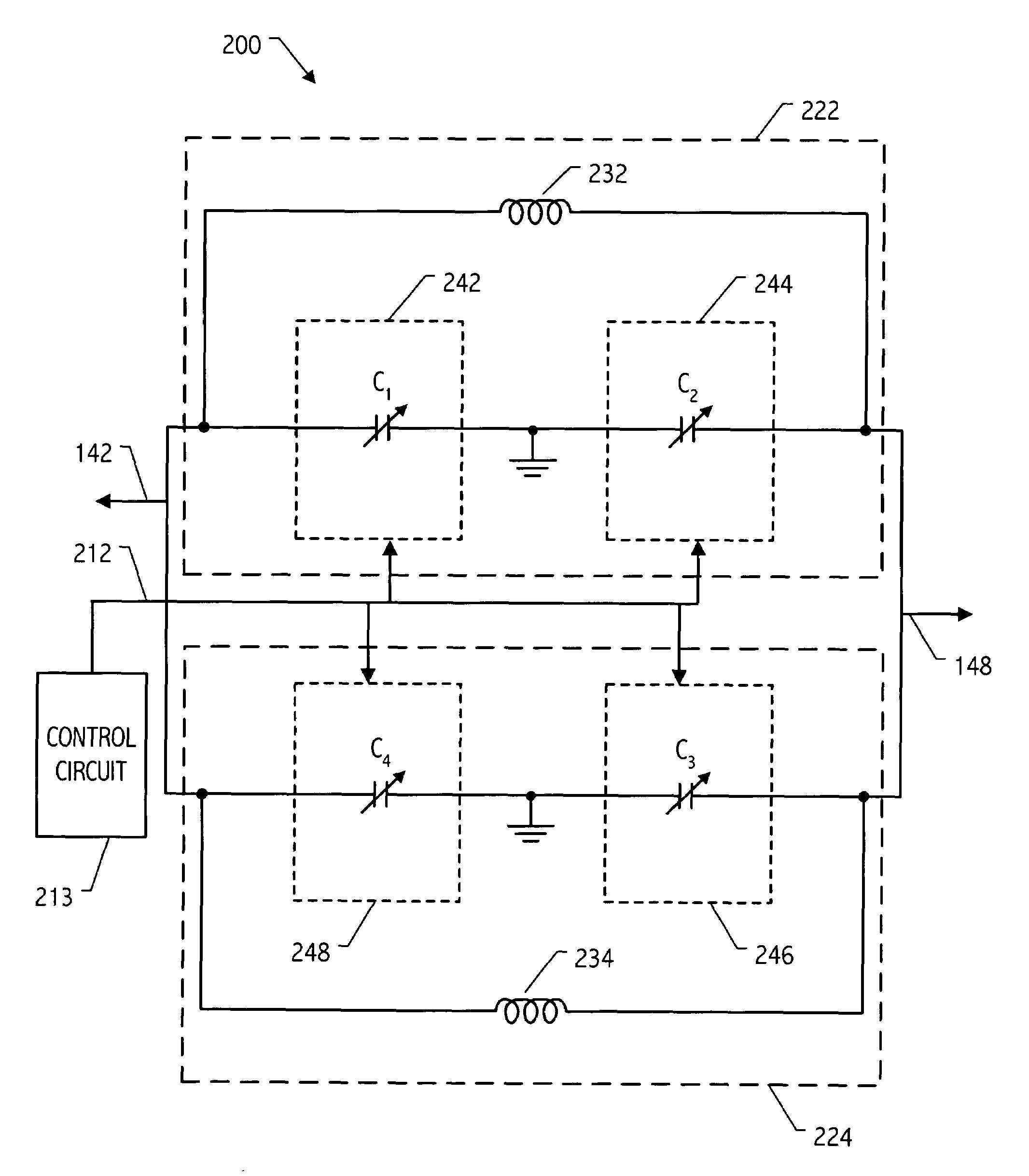
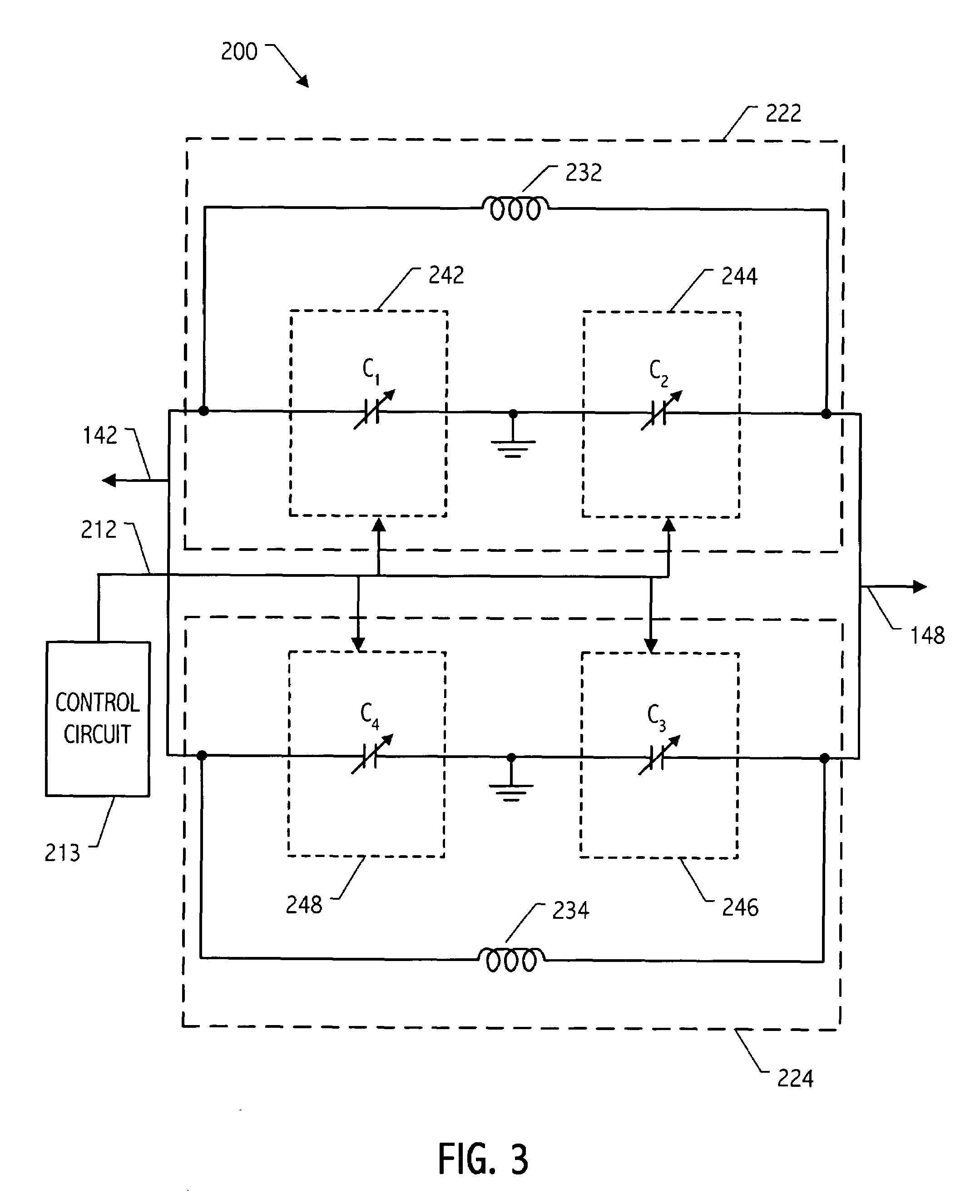
[0016]It has been discovered that a differential circuit may be controlled using differentially imbalanced control signals, for example, to improve control of gain and noise. For example, a capacitor array varactor including selectively enabled capacitors may be used to improve control of circuits and signals such as VCOs and VCO outputs. By implementing selectively enabled capacitors in a differential circuit environment, and by selectively enabling such capacitors in a non-fully-differential manner, greater control may be obtained without introducing an intolerable amount of differential noise.
[0017]Such a varactor is useful in implementing the PLL function found in clock and data recovery circuits, clock multiplication units, clock cleaning devices, etc., which advantageously incorporate multiple control signals to affect a frequency change. These analog (or digital) signals can change one control line (or one bit) at a time, and the single line which changes may be used to achieve a controlled transition time (or ramp rate) which is slow enough to cause a very gradual change in the value of the associated tuning elements. As a result, the PLL maintains lock during and after the digital signal changes state, and more importantly, maintains its phase accuracy so that the operation of the PLL, including subtle specifications such as input data jitter tolerance and jitter generation are not negatively impacted.

Problems solved by technology

However, such a discrete implementation is costly and requires a large amount of printed circuit board space, and more than likely would have difficulty achieving the performance required of modern systems while operating at an acceptable power level.
Consequently, most VCOs are implemented monolithically (i.e., on a single integrated circuit die).
While the frequency of the VCO can inherently be adjusted by an appropriate control voltage, the performance of the VCO may degrade if the control voltage otherwise necessary to achieve the desired VCO frequency falls too close to either the upper extreme or the lower extreme of its range.
In principle this would allow a PLL to compensate for a large deviation in VCO “center frequency” without requiring a control voltage dangerously close to “running out of range.” But there are detrimental consequences of increasing the VCO gain, including danger of locking onto a harmonic, and increased noise and jitter of the system.
Moreover, with most VCO circuit structures it is difficult to arbitrarily provide an ever higher and higher tuning range and still achieve good frequency and phase stability.
In either case, such trimming is a “permanent” adjustment of the center frequency during manufacture, but it adds costly manufacturing steps to either accomplish laser trimming after wafer fabrication or to provide a semiconductor process capable of implementing flash memory structures or other kinds of programmable structures.
Moreover, such trimming is performed once during manufacture, and cannot adjust for subsequent changes in environmental conditions that the circuit may be called upon to operate under.
Such storage elements are volatile and lose stored data when the circuit loses power.
These approaches are valuable additions to the state of the art, but they cannot accommodate variations in the center frequency as environmental conditions change, as semiconductor parameters drift over time (e.g., threshold voltage shifts), or as other artifacts of component aging occur.

Method used


Image

  • Imbalanced differential circuit control
  • Imbalanced differential circuit control
  • Imbalanced differential circuit control

Examples


Embodiment Construction

)

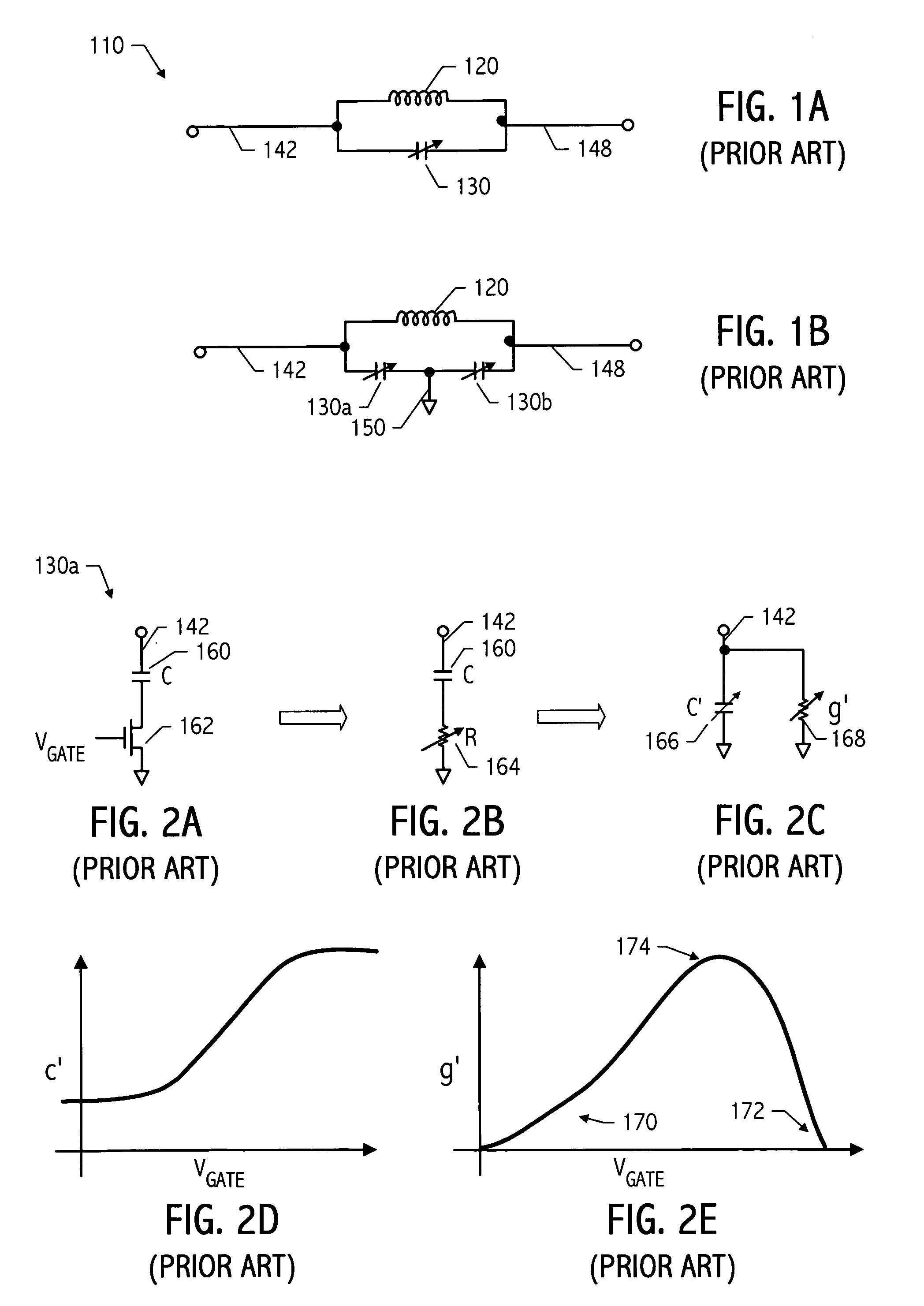
[0040]The following discussion is intended to provide a detailed description of at least one example of the invention to aid those skilled in the art to understand and practice the invention. For example, FIG. 1 and the following figures, and the discussion related thereto, describe at least one exemplary variable capacitance control system. This exemplary system provides a useful reference in discussing various aspects of the invention. Of course, the description of the system has been simplified for purposes of discussion, and it is just one of many different types of appropriate systems that may be used in accordance with the invention. Consequently, the following discussion should not be taken to be limiting of the invention itself. Rather, any number of variations may fall within the scope of the invention which is properly defined in the claims following this description.

[0041]FIG. 1A shows a resonant LC tank circuit 110 having a variable capacitor 130 coupled in parallel wit...


PUM


Abstract

A differential circuit includes first and second side circuits which are coupled to receive control signals in such a way as to introduce an intentional imbalance in the differential circuit for certain benefits discussed herein. An exemplary pseudo-differential LC tank circuit is described which includes first and second side nodes, and an inductance circuit and a variable capacitance circuit coupled between the nodes. The inductance and variable capacitance circuits may be broken out into separate tanks to achieve certain magnetic noise reduction benefits. Each exemplary variable capacitance circuit includes a first variable capacitance coupled between the first side node and a common ground node, and a second variable capacitance coupled between the second side node and the common ground. Each of the first and second variable capacitances is coupled to receive control lines for controlling the capacitance of the first and second variable capacitance circuits in a pseudo-differential manner. Each variable capacitance includes at least one of many types of switch-capacitor cells, some of which are described herein.

Description

CROSS-REFERENCE TO RELATED APPLICATION(S)[0001]This application claims priority to the following provisional patent applications which are hereby incorporated by reference in their entirety:[0002]U.S. provisional patent application Ser. No. 60 / 360,310, entitled “Digital-to-Analog Converter Circuit Incorporating Hybrid Sigma-Delta Modulator Circuit,” filed Feb. 28, 2002, and naming Yunteng Huang as inventor;[0003]U.S. provisional patent application Ser. No. 60 / 360,340, entitled “Optimal Control of a Capacitor Array Varactor for Improved Control of Gain and Noise,” filed Feb. 28, 2002, and naming Yunteng Huang as inventor; and[0004]U.S. provisional patent application Ser. No. 60 / 360,333, entitled “Digital Expander Apparatus and Method for Generating Multiple Analog Control Signals Particularly Useful for Controlling a Sub-Varactor Array of a Voltage Controlled Oscillator,” filed Feb. 28, 2002, and naming Yunteng Huang and Bruno Garlepp as inventors.BACKGROUND[0005]1. Field[0006]The pr...

Claims


Application Information

Patent Timeline
Patent Type & Authority Patents(United States)
IPC IPC(8): H03B5/12H03B5/18H03K3/282
CPCH03J3/20H03J2200/10
Inventor HUANG, YUNTENG
Owner XENOGENIC DEV LLC
Learn More