Method of manufacturing non-volatile DRAM

Inactive Publication Date: 2007-06-19
O2IC
View PDF53 Cites 16 Cited by
  • Summary
  • Abstract
  • Description
  • Claims
  • Application Information

AI Technical Summary

Benefits of technology

[0015]In accordance with the present invention, a method of forming a non-volatile DRAM in a semiconductor substrate, includes, in part, the steps of: forming at least two trench isolation regions in the semiconductor substrate, forming a first well between the two trench isolation regions, forming a second well between the two trench isolation regions and below the first well to define a body region, forming a first oxide layer above a first portion of the body region, depositing a first dielectric layer above the first oxide layer, depositing a first polysilicon layer above the first dielectric layer, depositing a second dielectric layer above the first polysilicon layer, depositing and patterning a first mask layer above the second dielectric layer to define a control gate of a non-volatile device of the non-volatile DRAM, etching the first oxide layer, the first dielectric layer, the first polysilicon layer and the second dielectric layer from all regions except those positioned below the first patterned mask layer, removing the first patterned mask layer, forming a first oxide spacer above portions of the body region and adjacent said first polysilicon layer, forming a second oxide layer above a second portion of the body region not covered by said first spacer, forming a third oxide layer above a third portion of the body region different from the second region and not covered by said first spacer, depositing a second polysilicon layer, depositing and

Problems solved by technology

Due to its larger memory cell size, an SRAM is typically more expensive to manufacture than a DRAM.
Therefore, where loss of data due to power failure or termination is unacceptable, a non-volatile memory is used to store the data.
Unfortunately, the non-volatile semiconductor memory is typically slower to operate than a volatile memory.
Furthermore, the non-volatile memory often requires a high voltage, e.g., 12 volts, to program or erase.
Such high voltages may cause a number of disadvantages.
The high voltage increases the power consumption and thus shortens the lifetime of the battery powering the memory.
The high voltage may degrade the ab

Method used


Image

  • Method of manufacturing non-volatile DRAM
  • Method of manufacturing non-volatile DRAM
  • Method of manufacturing non-volatile DRAM

Examples


Embodiment Construction

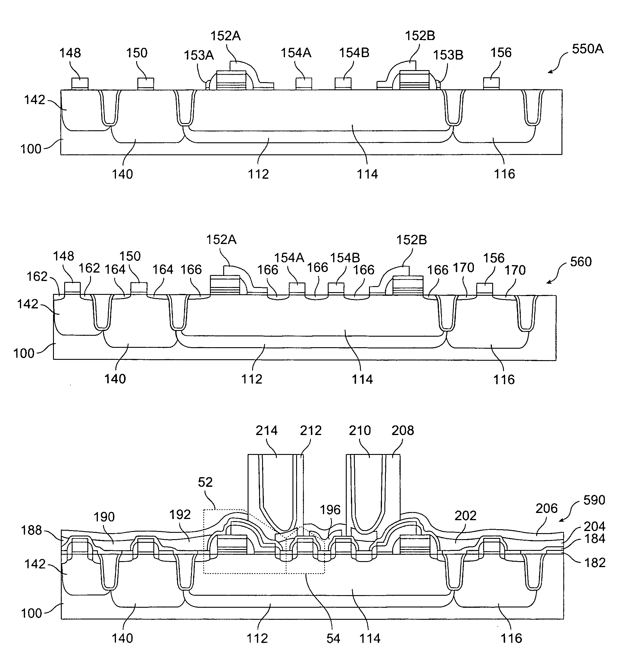
[0047]According to the present invention, an improved memory device and method is provided. More particularly, the invention provides a semiconductor memory that has integrated non-volatile and Dynamic random access memory cells. Although the invention has been applied to a single integrated circuit device in a memory application, there can be other alternatives, variations, and modifications. For example, the invention can be applied to embedded memory applications, including those with logic or microcircuits, and the like.

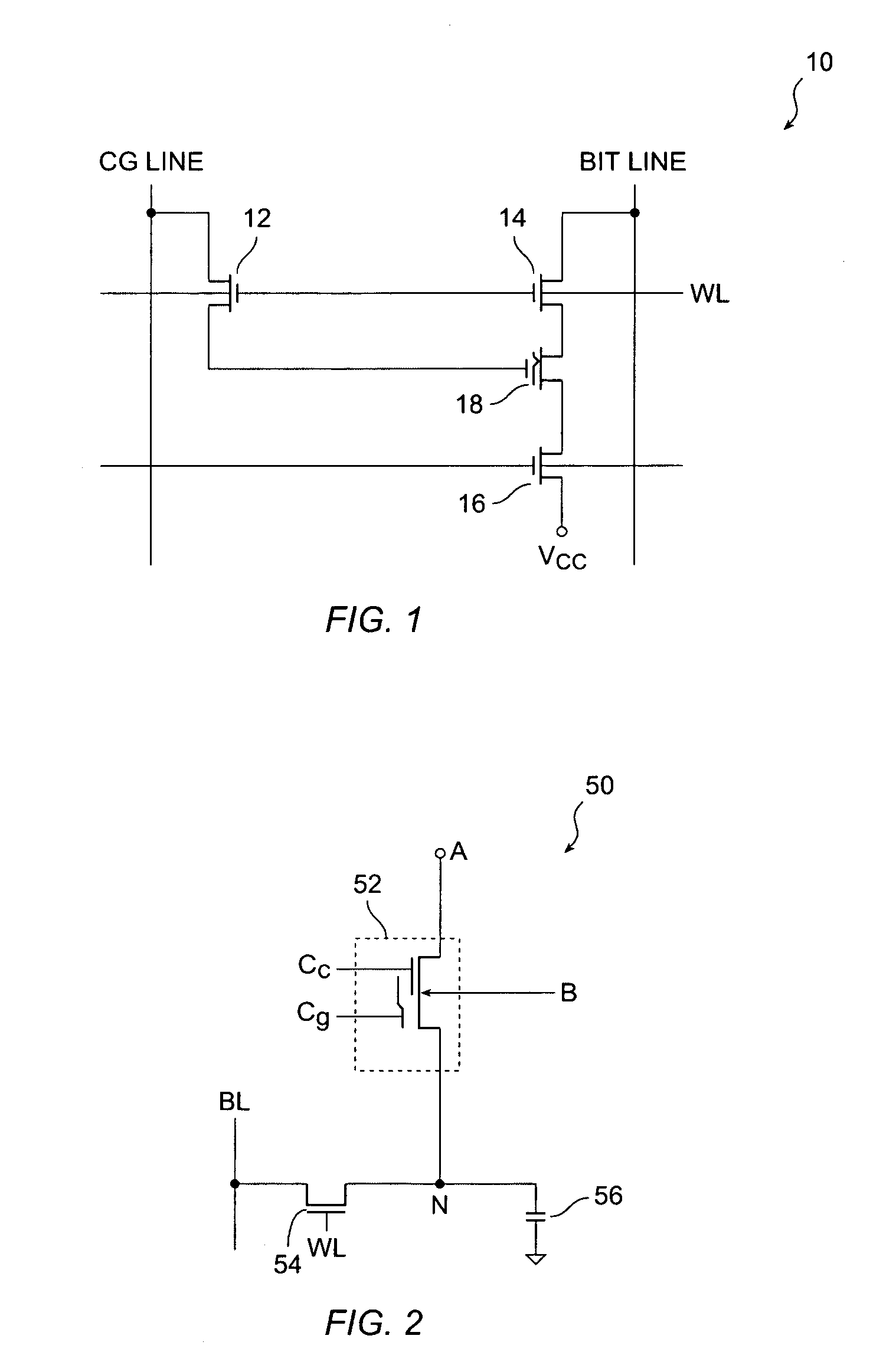
[0048]FIG. 2 is a transistor schematic diagram of a non-volatile dynamic random access memory (DRAM) 50. DRAM 50 includes non-volatile device 52, as well as MOS transistor 54 and capacitor 56 which together form a dynamic random access memory cell, in accordance with one embodiment of the present invention. This diagram is merely an example, which should not unduly limit the scope of the claims herein. One of ordinary skill in the art would recognize many other v...


PUM


Abstract

A method of forming a non-volatile DRAM includes, in part: forming p-well and an n-well between two trench isolation regions formed in a semiconductor substrate, forming a polysilicon control gate of the non-volatile device disposed in the non-volatile DRAM, forming a first oxide spacer above portions of the body region and adjacent said first control gate, forming gate oxide layers of varying thicknesses above the body region, forming the guiding gate of the non-volatile device and the gate of an associated passgate transistor, forming LDD implant regions of the non-volatile device and the associated pass-gate transistor, forming source/drain regions of the non-volatile device and the associated pass-gate transistor, depositing a dielectric layer over the polysilicon guiding gate of the non-volatile device and the polysilicon gate of the associated passgate transistor, forming polysilicon landing pads, and forming polysilicon vertical walls defining capacitor plates of the non-volatile DRAM capacitor.

Description

CROSS-REFERENCES TO RELATED APPLICATIONS[0001]The present application claims benefit of the filing date of U.S. provisional application No. 60 / 383,860 filed on May 28, 2002, entitled “Integrated RAM and Non-Volatile Memory” the entire content of which is incorporated herein by reference.[0002]The present application is related to copending application Ser. No. 10 / 447,715, entitled “Method Of Manufacturing Non-Volatile Memory Device”, filed contemporaneously herewith, assigned to the same assignee, and incorporated herein by reference in its entirety.[0003]The present application is related to copending application Ser. No. 10 / 394,417, filed on Mar. 19, 2003, entitled “Non-Volatile Memory Device”, assigned to the same assignee, and incorporated herein by reference in its entirety.STATEMENT AS TO RIGHTS TO INVENTIONS MADE UNDER FEDERALLY SPONSORED RESEARCH OR DEVELOPMENT[0004]NOT APPLICABLEREFERENCE TO A “SEQUENCE LISTING,” A TABLE, OR A COMPUTER PROGRAM LISTING APPENDIX SUBMITTED ON ...

Claims


Application Information

Patent Timeline
IPC IPC(8): H01L21/8244
CPCH01L27/105H01L27/10873H01L27/10894H01L27/115H01L27/11521H01L27/1052H10B99/00H10B12/05H10B12/09H10B69/00H10B41/30
Inventor CHOI, KYU HYUNLI, SHEAU-SUEY
Owner O2IC
Why Eureka
Try Eureka