Image inputting device

a technology of inputting device and image, which is applied in the direction of paper-money testing device, fluorescence/phosphorescence, instruments, etc., can solve the problems of reducing the merits obtained by automatic detection of process, reducing the size of the mail and the device, and reducing the number of components. , the effect of reducing the number of components

Active Publication Date: 2007-06-26
NEC CORP
View PDF8 Cites 3 Cited by
  • Summary
  • Abstract
  • Description
  • Claims
  • Application Information

AI Technical Summary

Benefits of technology

[0023]In view of the above, it is a first object of the present invention to provide an image inputting device capable of reducing costs for its manufacturing and of simply performing adjustment processing and reliable and speedy detection of an indicia even in the case of nonstandard size postal matter. It is a second object of the present invention to provide an image inputting device capable of contributing to miniaturization of an indicia detection processing module and to reduction in costs for manufacturing the image inputting device.
[0040]With the above configuration, fluorescence or phosphorescence can be received from an entire surface of a object and, therefore, even if the object has large variations in size, reliable and speedy detection can be made in a light emitting area. A light radiation limiting unit is provided which enables a fluorescence image and a phosphorescence image to be reliably obtained.
[0041]With another configuration as above, since the fluorescence and phosphorescence can be received from an entire object, unlike in the conventional case, repeated detection processing in a light emitting area by reversing a object is not required, thus, contributing to miniaturization of the image inputting device and reduction in costs for manufacturing the same.
[0043]With still another configuration as above, by using a linear CCD array as a sensor making up the detecting unit, costs can be reduced and an adjusting operation can be performed easily.
[0044]With still another configuration as above, the ultraviolet light LED is used as the light source and, by making the light source be flashed, fluorescence is received during radiating period and phosphorescence is received during non-radiating period, an fluorescence image and phosphorescence image can be detected in a same field of view and a same optical axis can be used and, therefore, the number of components can be reduced almost to a half, thus achieving miniaturization and cost reduction.

Problems solved by technology

On the other hand, in the case of nonstandard size postal matter, there are many problems such as a difficulty in handling mail and device sizes, and in processing capability and, therefore, automatization (mechanization) for handling the nonstandard size postal matter is not yet advancing.
Thus, a problem occurs when the conventional culling-facing-canceling machine for letters is used as the culling-facing-canceling machine to be applied to nonstandard size postal matter.
Moreover, another problem occurs, for example, in that a plurality of numbers of stamps can be detected so long as the postage stamps are placed along a carrying direction, however, an omission occurs in the detection of stamps if being arranged in a longitudinal direction (vertical and scanning direction) orthogonal to a carrying direction, which, as a result, causes a decrease of merits obtained by making the detecting processes automatic.
However, this proposal has also a problem in that the photosensors can be arranged only at intervals of about 20 mm at most, due to a limitation in terms of a physical size, making it impossible to improve resolution of the photosensors and difficult to accurately detect the kind or position of the indicia.
Another problem is that, to solve a problem of variations in thickness of postal matter, an adjustment of overlapping between areas for detection by the photosensors and / or compensation for variations in sensitivity among the photosensors are required.
Still another problem is that, even if a single photosensor is employed, an adjustment of a gain and / or offset of the photosensor is needed and, if the plurality of the photosensors is used in combination, the adjustment is made complicated, causing much time and labor to be required.
Still another problem is that use of many photosensors causes high costs.
A first problem to be solved is that, when the postal matter is radiated with the ultraviolet light and, as a result, the phosphorescence or fluorescence is received from the indicia, it is difficult to receive the phosphorescence, which is emitted with delay separately from the emission of the fluorescence, in a state in which the phosphorescence is differentiated from the fluorescence, thus making it impossible to accurately detect a kind or position of the indicia of the postal matter.
A second problem to be solved is that, if such a feed-back path as employed in the conventional culling-facing-canceling machine for letters or such an additional pair of the image inputting devices is provided also on a downstream side as employed in the culling-facing-canceling machine for letters, the indicia detection processing module is made larger due to the large postal matter, which causes costs to be increased and a limitation to be imposed on an installation place.

Method used


Image

  • Image inputting device
  • Image inputting device
  • Image inputting device

Examples


first embodiment

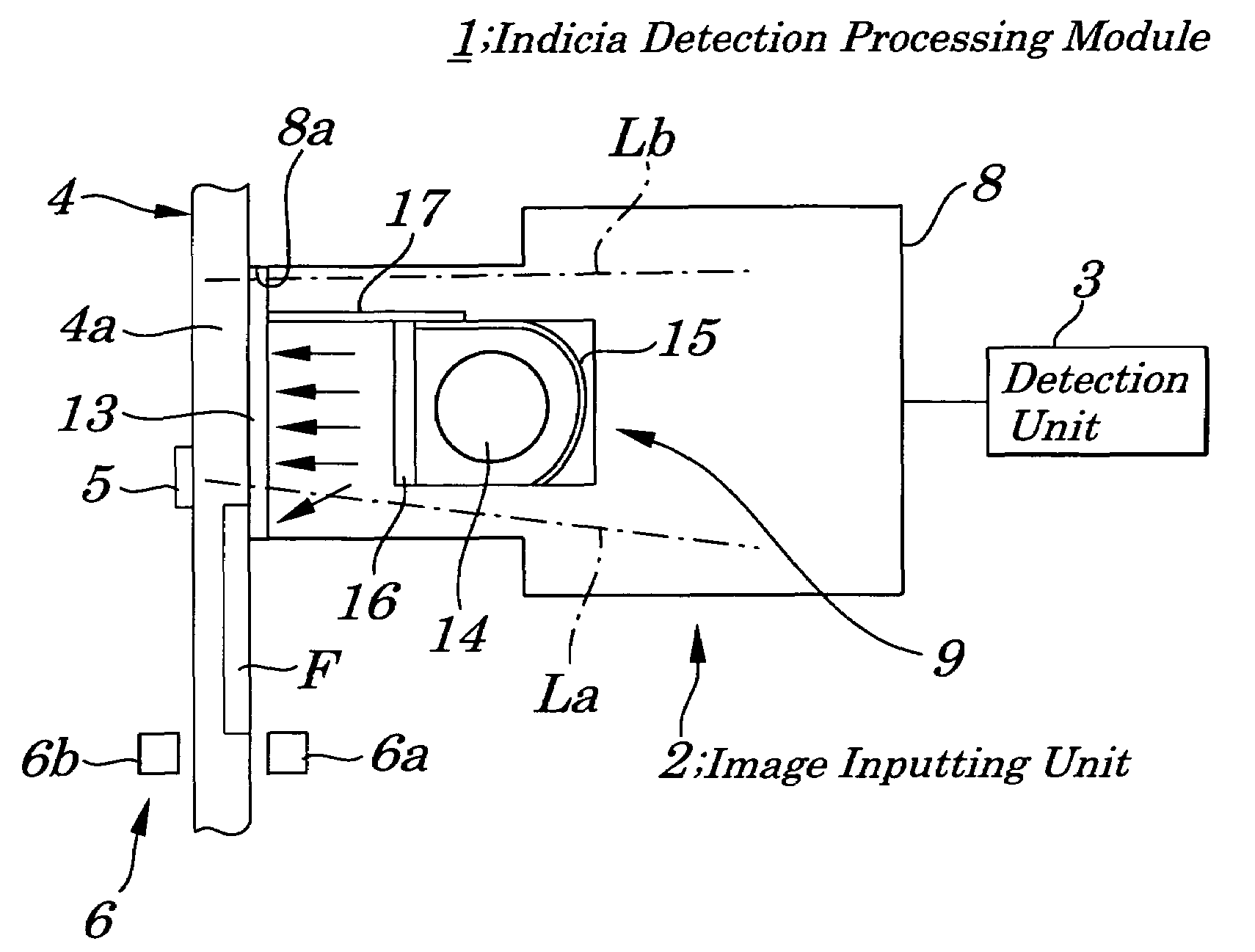
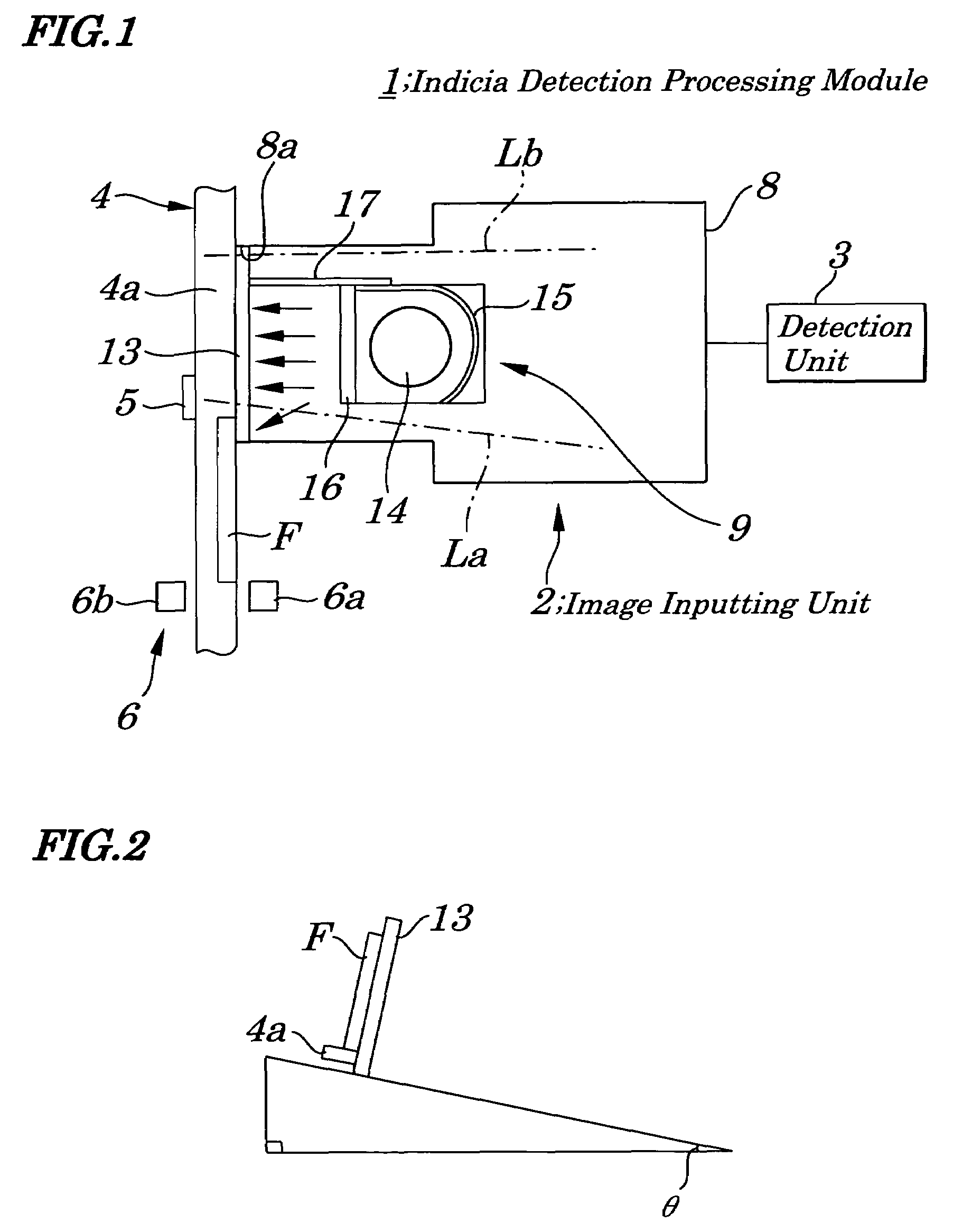
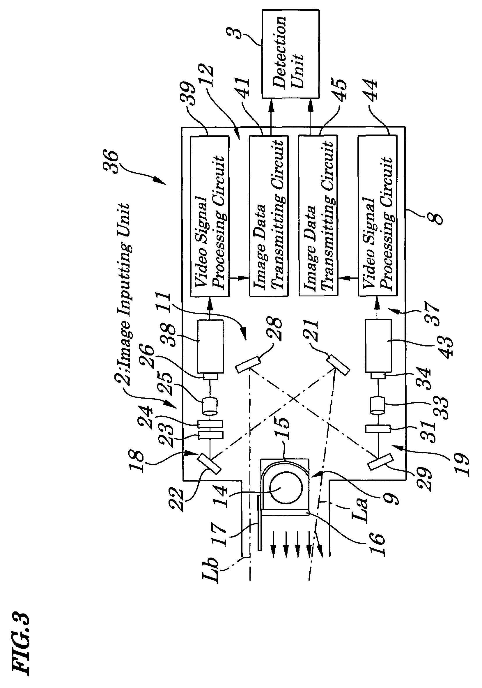
[0064]FIG. 1 is a diagram schematically illustrating configurations of an indicia detection processing module 1 of a first embodiment of the present invention. FIG. 2 is a diagram explaining configurations of the indicia detection processing module 1 of the first embodiment. FIG. 3 is a diagram schematically illustrating configurations of the indicia detection processing module of the first embodiment. FIG. 4 is a diagram showing an example of an image to be captured by detecting units making up the indicia detection processing module 1 of the first embodiment.

[0065]The indicia detection processing module 1 of the embodiment includes an image inputting unit 2 making up a culling-facing-canceling machine for nonstandard size postal matter (flat mail) to make an nonstandard size postal matter “F” be radiated with ultraviolet light and to receive fluorescence and phosphorescence from an indicia, such as a postage stamp, a permit imprint, a meter (postage paid) or a like affixed to and ...

second embodiment

[0089]FIG. 5 is a diagram schematically illustrating configurations of an indicia detection processing module according to a second embodiment of the present invention. The configurations of the indicia detection processing module of the second embodiment differs from those of the first embodiment in that a phosphorescence receiving optical system is not so configured that it can receive two phosphorescence emitting colors (for example, green and red colors) emitted from an indicia unlike in the conventional case where the indicia detection processing module can receive one single phosphorescence emitting color (for example, green color only). Configurations other than those described above are the same as those in the first embodiment and their descriptions are omitted accordingly.

[0090]An image inputting unit 51 employed in the indicia detection processing module of the second embodiment includes a housing 8, a light radiating section 9, a light receiving section 52 to receive flu...

third embodiment

[0095]FIG. 6 is a diagram schematically illustrating configurations of an indicia detection processing module 71 of a third embodiment of the present invention. FIG. 7 is a diagram schematically showing configurations of an indicia detection processing module of the third embodiment. FIG. 8 is a time chart explaining operations of the indicia detection processing module of the third embodiment. The indicia detection processing module of the third embodiment differs from those of the first embodiment in that an ultraviolet light LED (Light Emitting Diode) is used as a light source, instead of an ultraviolet fluorescent lamp, and receives fluorescence or phosphorescence on a same optical path by turning ON / OFF an ultraviolet light LED and fluorescence and phosphorescence images are detected according to timing of the ON / OFF operations. Configurations other than those described above are the same as those in the first embodiment and their descriptions are omitted accordingly.

[0096]The ...


PUM

PropertyMeasurementUnit
thicknessaaaaaaaaaa
heightaaaaaaaaaa
sizeaaaaaaaaaa

Abstract

An image inputting device is provided which is capable of making reliable and speedy detection of an indicia even for an nonstandard size postal matter. The postal matter, when having passed by a proximity detecting section, is radiated with ultraviolet light at specified timing from light radiating unit. When a postal matter is radiated with ultraviolet light, fluorescence is emitted from a phosphor formed on an indicia after being pumped. In the case where the indicia is an meter, when the meter passes by a fluorescence field of view, red fluorescence enters a fluorescence light receiving optical system along a fluorescence detecting optical axis. If the indicia is a postage stamp containing a substance that emits phosphorescence, when the postage stamp passes by a phosphorescence detecting field of view where no ultraviolet light is not emitted, green fluorescence enters a phosphorescence light receiving optical system along a phosphorescence detecting optical axis.

Description

BACKGROUND OF THE INVENTION[0001]1. Field of the Invention[0002]The present invention relates to an image inputting device being preferably used in, for example, a culling-facing-canceling machine for postal matter, and more particularly to the image inputting device for detecting and identifying a type, position, amount, and / or a like of an indicia, such as a postage stamp, a permit imprint, a meter, and / or a like, affixed or printed on a nonstandard size mail (flat mail).[0003]The present application claims priority of Japanese Patent Application No. 2004-020570 filed on Jan. 28, 2004, which is hereby incorporated by reference.[0004]2. Description of the Related Art[0005]Conventionally, in order to cancel postage stamps and / or face standard size mails (letter mails) including postcards, a culling-facing-canceling machine to be exclusively used for letters has been developed and is in actual use.[0006]The culling-facing-canceling machine 101 for letters, as shown in FIG. 9, include...

Claims


Application Information

Patent Timeline
Patent Type & Authority Patents(United States)
IPC IPC(8): G01N21/64B07C3/14G07D7/00G06T1/00G07B17/00G07D7/12H04N7/18
CPCG07D7/122G07B2017/00709G07D7/1205
Inventor WATANABE, MITSURUSINGU, SATOSHIUNO, KOEI
Owner NEC CORP
Why Eureka
Try Eureka