Wide bandgap semiconductor device construction

Inactive Publication Date: 2007-07-10
MICROSEMI
View PDF17 Cites 6 Cited by
  • Summary
  • Abstract
  • Description
  • Claims
  • Application Information

AI Technical Summary

Benefits of technology

[0007]In view of the foregoing, a primary object of the present invention is to provide improved methods of constructing wide bandgap semiconductor devices. Another object of the present invention is to improve material etching during the construction of wide bandgap semiconductor devices.
[0009]In this regard, one or more of the above objectives and additional advantages may be realized by a first aspect of the present invention, which provides a method for precisely etching a wide bandgap semiconductor device. The method includes, in a wide bandgap semiconductor device including a first and second semiconductor material layer, measuring a conductance of a layer of interest, etching a first amount of material from the layer of interest, measuring a second conductance of the layer of interest, and using the measured conductance to determine an etch time to remove a second amount of material from the layer of interest.
[0012]According to another embodiment of the present invention, the method may further include the step of, prior to measuring the conductance, isolating an area of the layer of interest for locating a conductance measurement device. According to this characterization, the conductance measurement device may be a probe device that utilizes a current provided through a first pair of probes, while a second pair of probes reads a voltage drop created across the layer of interest, from which, a layer conductance (C) may be calculated using the relationship between current, voltage, and conductance, e.g. conductance=current / voltage. Advantageously, the present isolation step improves the accuracy of the conductance measurement by minimizing current leakage and the influence of other features, such as emitter mesas in close proximity and / or defects in the semiconductor material.

Problems solved by technology

While the potential of SiC is recognized, appropriate techniques for producing devices is lacking, because the requirements of specific devices are often difficult to achieve using SiC.
Furthermore, such devices require careful control of the conductivity and thickness of the layers to achieve desired oscillation frequencies and power gains.
Unfortunately, however, conventional SiC etching methods do not always result in uniform etch times, even where the layer thickness is known, thereby making it difficult to accurately control etching during device construction.

Method used


Image

  • Wide bandgap semiconductor device construction
  • Wide bandgap semiconductor device construction
  • Wide bandgap semiconductor device construction

Examples


Embodiment Construction

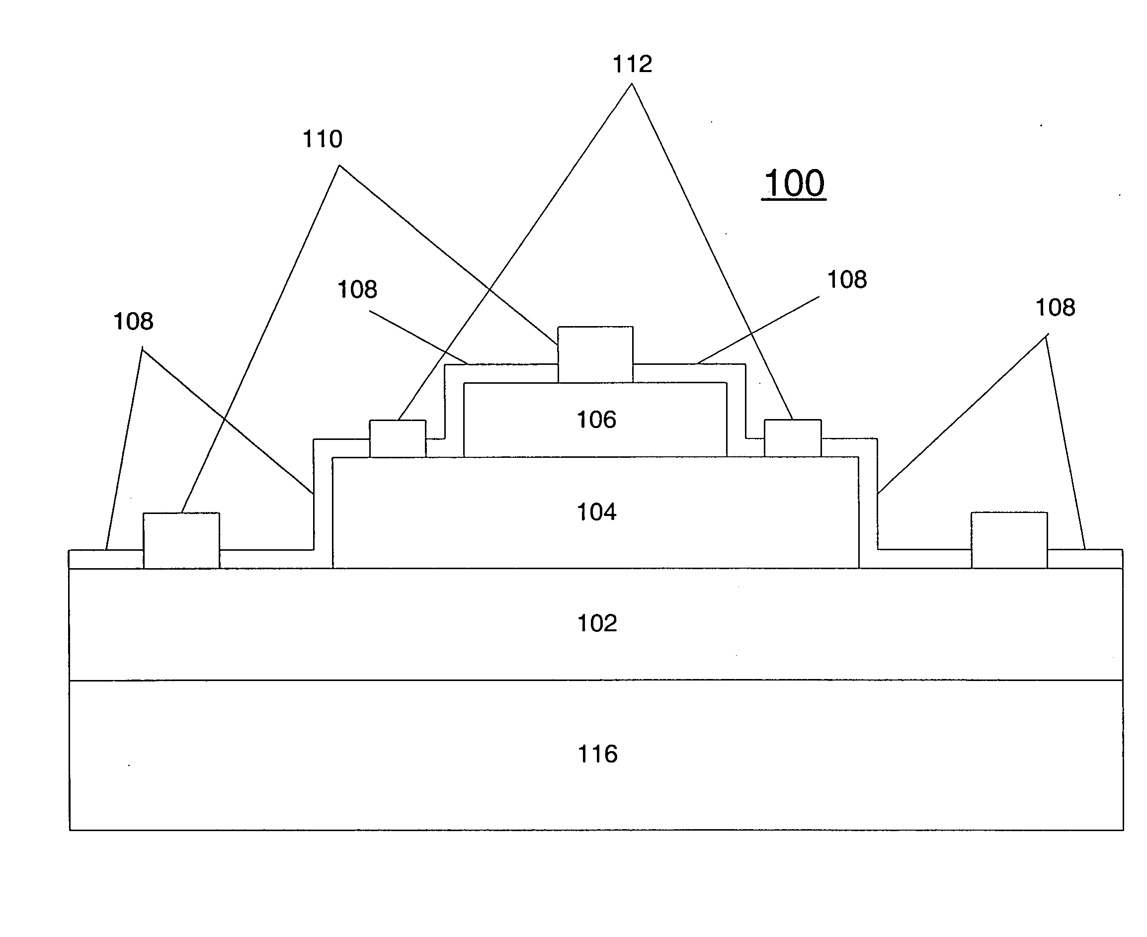
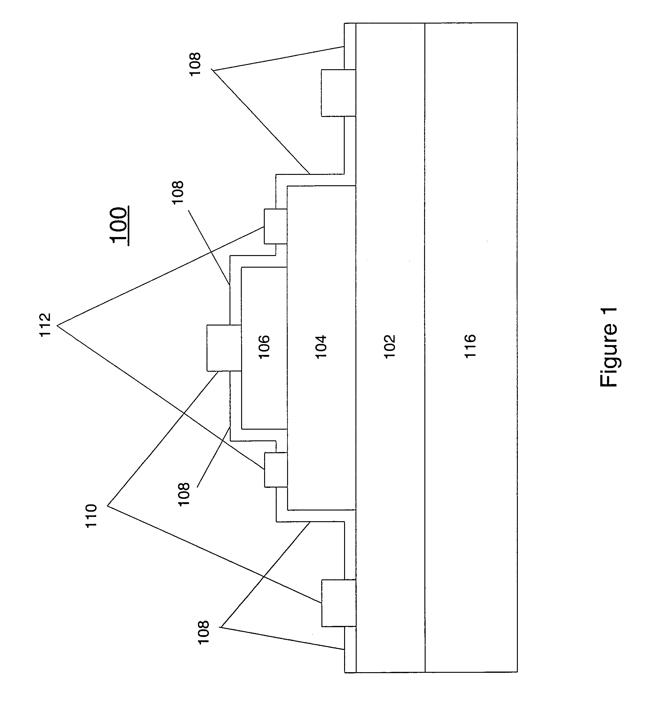
[0025]Reference will now be made to the accompanying drawings, which at least assist in illustrating the various pertinent features of the present invention. In this regard, the following description is presented for purposes of illustration and description and is not intended to limit the invention to the form disclosed herein. Consequently, variations and modifications commensurate with the following teachings, and skill and knowledge of the relevant art, are within the scope of the present invention. The embodiments described herein are further intended to explain the best modes known of practicing the invention and to enable others skilled in the art to utilize the invention in such, or other embodiments and with various modifications required by the particular application(s) or use(s) of the present invention. As such, the following description sets forth an exemplary SiC BJT structure and associated processes that involve regrowth, self-alignment, and other features and advant...


PUM


Abstract

The invention includes methods for precisely and accurately etching layers of wide bandgap semiconductor material. According to one aspect of the invention, the method includes providing a multi-layer laminate including at least a first and second layer of wide bandgap semiconductor material, measuring a first conductance of the first layer of semiconductor material, partially etching the first layer of semiconductor material a first amount, measuring a second conductance of the first layer of semiconductor material etched the first amount, and utilizing the first and second measured conductance to determine a time required to etch the first layer of semiconductor material a second amount.

Description

RELATED APPLICATIONS[0001]This patent application claims priority from U.S. Patent Application Ser. No. 60 / 399,957, that was filed on Jul. 30, 2002, and that is entitled “SILICON CARBIDE BIPOLAR JUNCTION TRANSISTOR FABRICATION PROCESSES.” The entire disclosure of U.S. Patent Application Ser. No. 60 / 399,957 is incorporated herein by reference.GOVERNMENT INTERESTS[0002]At least a portion of the work related to the invention described herein was made in the performance of work under a Government contract No. N00014-99-C-0332. All rights possessed by the U.S. Government in this subject matter are governed by the terms of that contract.FIELD OF THE INVENTION[0003]The present invention generally relates to wide bandgap semiconductor devices, and in particular, to methods of constructing the same.BACKGROUND OF THE INVENTION[0004]Wide bandgap semiconductor devices are devices constructed from wide bandgap materials, e.g. generally having an energy gap greater than 2.5 eV, such as Silicon Ca...

Claims


Application Information

Patent Timeline
IPC IPC(8): H01L21/302H01L21/04H01L21/331H01L21/66H01L29/20
CPCH01L21/0445H01L29/66068H01L29/66318H01L22/20H01L29/2003
Inventor VAN ZEGHBROECK, BART J.PEREZ, IVANTORVIK, JOHN T.
Owner MICROSEMI
Why Eureka
Try Eureka