Photonic crystal structure for mode conversion

a technology of mode conversion and crystal structure, which is applied in the direction of optical waveguide light guide, instruments, nanotechnology, etc., can solve the problems of affecting the quality of optical components, the inability to equip such lasers with mode converters, and the substantial increase in size and hence the cost of components, so as to achieve short optic transitions and low losses

Inactive Publication Date: 2007-07-10
CENT NAT DE LA RECHERCHE SCI
View PDF24 Cites 21 Cited by
  • Summary
  • Abstract
  • Description
  • Claims
  • Application Information

AI Technical Summary

Benefits of technology

[0033]The propagation structure of the invention advantageously makes it possible to achieve short optic transitions with very low losses.

Problems solved by technology

They are detrimental for example for circuit fabrication, in particular circuits which have to reach good dynamic performance levels.
It is therefore not possible to equip such laser with a mode converter of known art.
Also a non-negligible quantity of material is needed to fabricate these converters, which leads to a substantial increase in size and hence the costs of components.

Method used


Image

  • Photonic crystal structure for mode conversion
  • Photonic crystal structure for mode conversion
  • Photonic crystal structure for mode conversion

Examples


Embodiment Construction

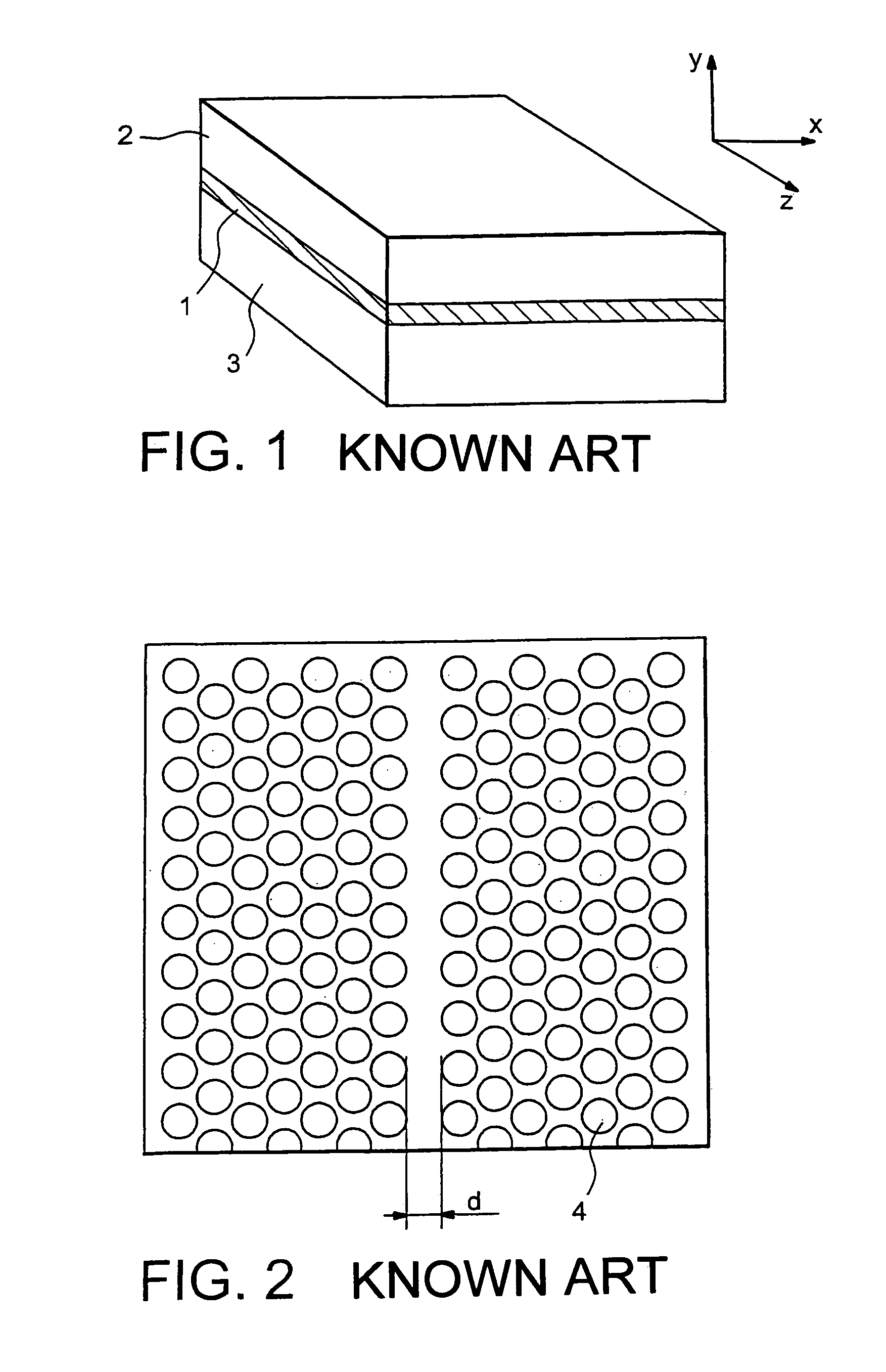
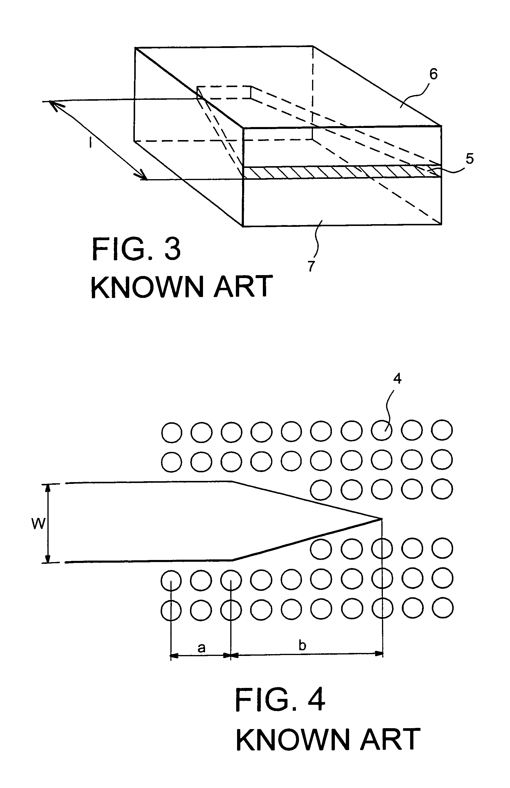
[0052]FIGS. 1, 2, 3, 4 and 5 have been previously described and do not require further description.

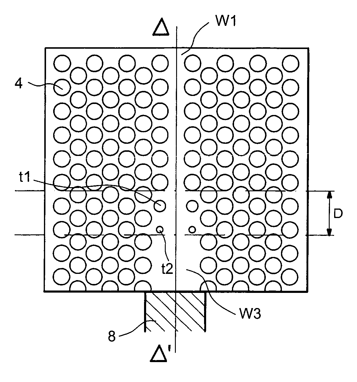
[0053]FIG. 6 is an overhead view of a first example of mode converter according to the invention. The mode converter is made in a photonic crystal structure consisting of a set of patterns 4. Patterns 4 are, for example, air holes obtained by etching a semiconductor material. The vertical confinement of the propagating wave is ensured by a layer of high index (GaInAsP) the thickness of which is, for example, 500 nm, positioned between two layers of material with a lower index (InP). The air-holes are positioned in the direction of wave propagation and for example define a triangular lattice whose mesh size is 450 nm. The diameter of the holes may be 300 nm for example with a depth of 1 μm. Isotropic etching, for example plasma dry etching, is used to make the holes. The converter operates the conversion of a W1 guide mode into a W3 guide mode and reciprocally.

[0054]Guide part W1 is cha...


PUM


Abstract

A photonic crystal guided propagation structure. The structure includes a guide portion Wn, n being a positive real number or zero number, having a first configuration of rows of patterns, and a guide portion Wm, m being a real number, m>n, having a second configuration of rows of patterns, and a transition zone of distance D located between guide portion Wn and guide portion Wm, in which patterns aligned with at least one row of patterns in the first configuration decrease in size over distance D to allow progressive passing from the first configuration of rows of patterns to the second configuration of rows of patterns. The structures can be applied to the area of integrated optics (semiconductor lasers, laser modulators, filters, multiplexors, etc.).

Description

CROSS REFERENCE TO RELATED APPLICATIONS[0001]This application is filed under 35 U.S.C. §371 for PCT / FR02 / 03993, filed Nov. 21, 2002, and is based upon and claims priority under 35 U.S.C. §119 from French Patent Application No. 0115057, filed Nov. 21, 2001.BACKGROUND OF THE INVENTION[0002]The present invention concerns a photonic crystal structure for mode conversion.[0003]The invention applies to the area of integrated optics.[0004]In known art, the function of a mode converter or transformer is to convert a first optic mode which propagates in a first guided propagation structure into a second optic mode able to propagate in a second guided propagation structure. The two guided propagation structures may either form part of one same photonic integrated circuit, or form part of two separate circuits. A guided propagation structure may, for example, be an optic fibre.[0005]FIG. 1 shows a guided propagation structure with vertical confinement of known art. Light propagates in directio...

Claims


Application Information

Patent Timeline
Patent Type & Authority Patents(United States)
IPC IPC(8): G02B6/10G02B6/26G02B6/42G02B6/12G02B6/122G02B6/14
CPCB82Y20/00G02B6/1225G02B6/14
Inventor TALNEAU, ANNE JULIETTELALANNE, PHILIPPE
Owner CENT NAT DE LA RECHERCHE SCI
Why Eureka
Try Eureka