Peeling method and method for manufacturing display device using the peeling method

a technology of peeling and manufacturing display devices, applied in the direction of identification means, instruments, optics, etc., to achieve the effects of reducing cost, reducing yield, and simplifying the curing of adhesives for transferring

Inactive Publication Date: 2007-07-17
SEMICON ENERGY LAB CO LTD
View PDF45 Cites 49 Cited by
  • Summary
  • Abstract
  • Description
  • Claims
  • Application Information

AI Technical Summary

Benefits of technology

[0027]A peeling process repeating the removal and curing of the adhesive for transferring can be simplified by using the peeling methods. Therefore, in the peeling process of the present invention, it can be formed with a preferable yield since an entire peel-off layer can be peeled. By peeling an entire peel-off layer, plural semiconductor elements can be formed on one large-size substrate and a gang printing which cut the substrate every semiconductor device can be performed; thereby cost reduction can be expected. In addition, the first substrate and the like can be recycled; thereby a low cost display device can be achieved to utilize far more inexpensive film substrate.
[0028]As a result, a light emitting device, a liquid crystal display device and other display device having the TFT or the like are made thin, hard to damage even in be

Problems solved by technology

However, there were a lot of problems in the aforementio

Method used


Image

  • Peeling method and method for manufacturing display device using the peeling method
  • Peeling method and method for manufacturing display device using the peeling method
  • Peeling method and method for manufacturing display device using the peeling method

Examples


embodiment mode 1

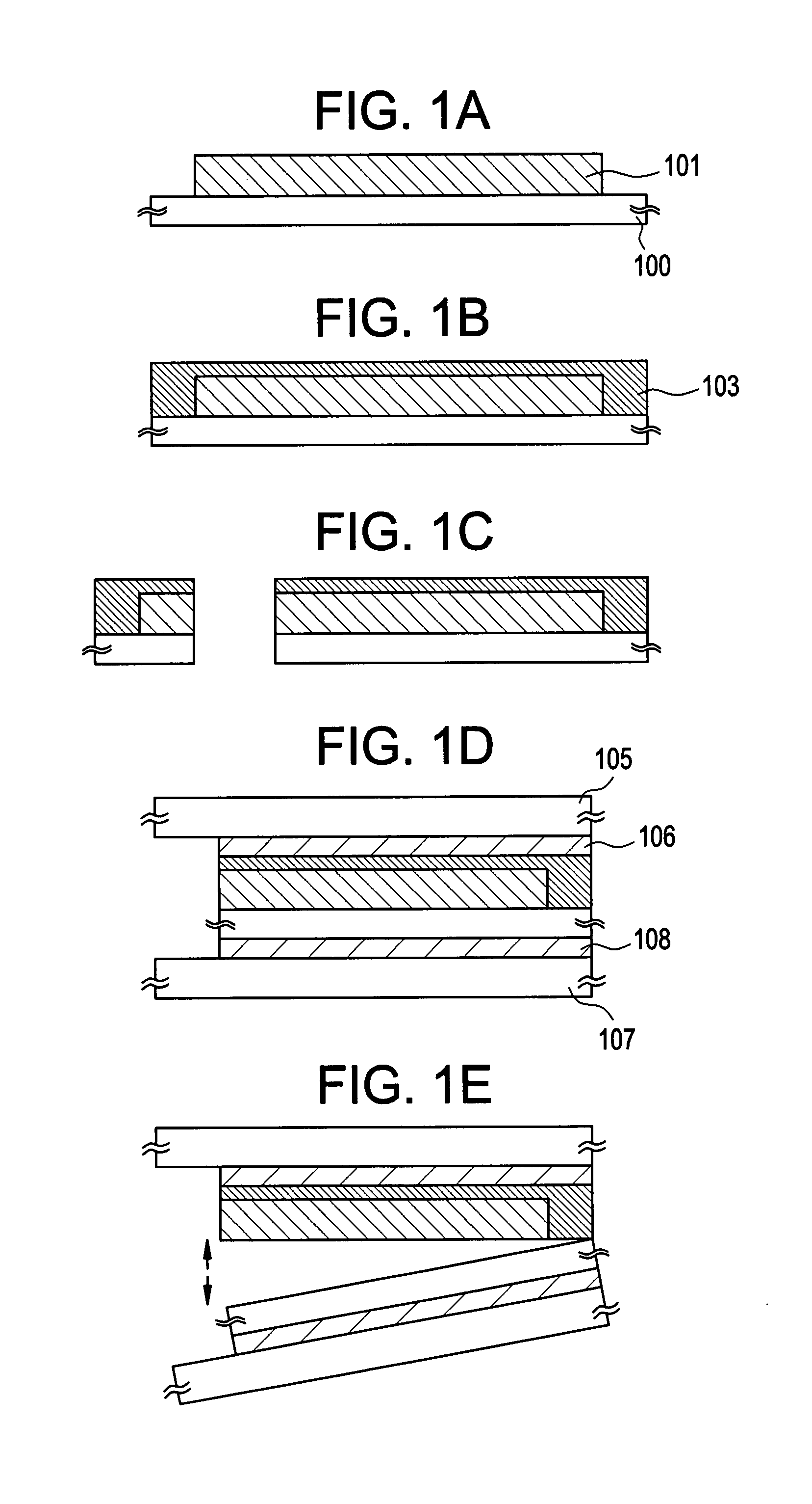
[0046]In the present embodiment mode, a peel-off layer is in a state in which up to a light emitting element and a liquid crystal element are formed, and an example of a specific peeling process in the case of performing peeling and transferring and of forming a top emission light emitting device according to the peeling process of the present invention is described.

[0047]As shown in FIG. 3(A), a metal film 201 is formed on a first substrate 200. In the embodiment mode, a glass substrate with a film thickness of approximately 0.5 to 1.0 mm is utilized for the first substrate. As for the metal film, a monolayer or a lamination layer comprising an alloy material or a compound material of W, Ti, Ta, Mo, Nd, Ni, Co, Zr, Zn, Ru, Rh, Pd, Os and Ir or containing the element as its main component can be used. Sputtering may be used as a manufacturing method for the metal film on the first substrate using metal as a target. In addition, a film thickness of the metal film is 10 nm to 200 nm, ...

embodiment mode 2

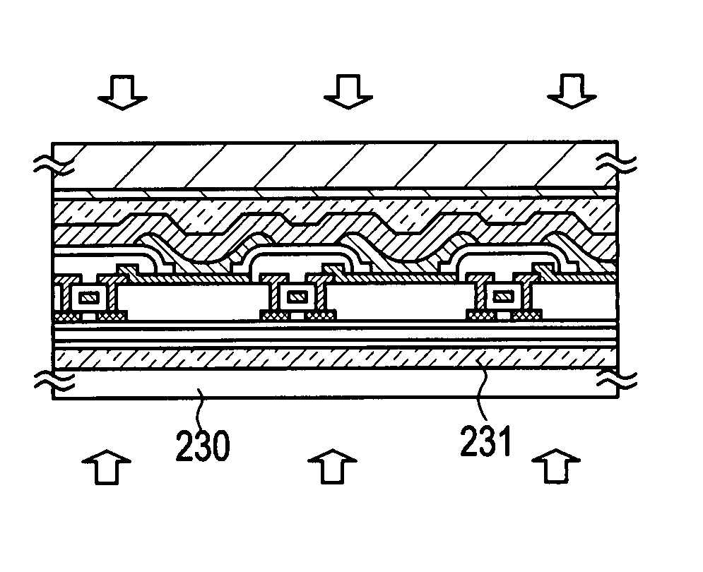
[0078]In the present embodiment mode, a peel-off layer is in a state in which up to a light emitting element and a liquid crystal element are formed. A case of performing peeling and transferring, that is, an example of manufacturing a bottom emission light emitting device by using a peeling process of controlling adhesiveness of an adhesive by adding an ultraviolet ray and heat is described. In addition, description of process or materials as in the embodiment mode 1 is omitted.

[0079]At first, to a protective film 215 are formed as the embodiment mode 1 (FIG. 4(A)). However, it is necessary to use a material having light-transmitting properties for a electrode 204 because it is a bottom emission light emitting device. In addition, although a stress relaxation material may be provided, it is not particularly provided in the present embodiment mode.

[0080]Next, as shown in FIG. 4(B), a second substrate 220 is fixed on the protective film 215 using a two-sided tape as an adhesive, then...

embodiment mode 3

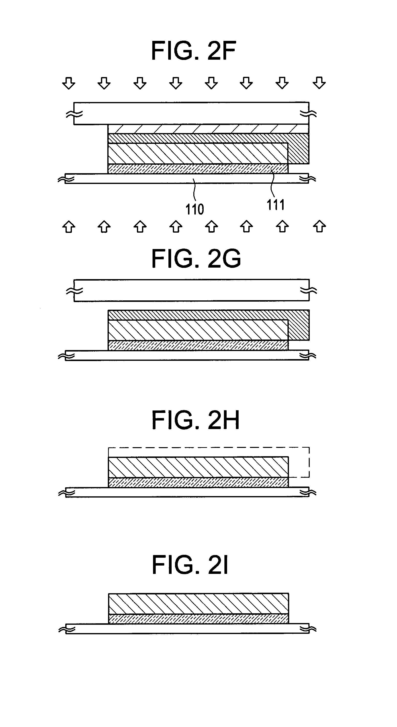
[0086]In the present embodiment mode, a peel-off layer is in a state in which up to a semiconductor element, an electrode, an insulating film and the like are formed, and a method for manufacturing a light emitting device when peeling and transferring are performed is described.

[0087]As shown in FIG. 12(A), a metal film 201 is formed on a first substrate 200. In the present embodiment mode, a glass substrate with a thickness of about 0.5 to 1.0 mm is utilized. As for the metal film, a monolayer or a lamination layer comprising an alloy material or a compound material of W, Ti, Ta, Mo, Nd, Ni, Co, Zr, Zn, Ru, Rh, Pd, Os and Ir or containing the element as its main component can be used. The metal film may be formed over the first substrate by sputtering using metal as a target. Note that the film thickness of the metal film shall be 10 nm to 200 nm, preferably be 50 nm to 75 nm.

[0088]When a metal alloy of the aforementioned metal (for example, an alloy of W and Mo: WxMo1-x) is used f...


PUM


Abstract

The present invention provides a simplifying method for a peeling process as well as peeling and transcribing to a large-size substrate uniformly. A feature of the present invention is to peel a first adhesive and to cure a second adhesive at the same time in a peeling process, thereby to simplify a manufacturing process. In addition, the present invention is to devise the timing of transcribing a peel-off layer in which up to an electrode of a semiconductor are formed to a predetermined substrate. In particular, a feature is that peeling is performed by using a pressure difference in the case that peeling is performed with a state in which plural semiconductor elements are formed on a large-size substrate.

Description

TECHNICAL FIELD[0001]The present invention relates to a peeling method of a functional thin film, specifically relates to a peeling method of a film or a layer having various elements. In addition, the present invention relates to a transferring method for pasting a peeled film to a film substrate, a semiconductor device and method for manufacturing thereof having a thin film transistor (hereinafter, referred to as a TFT) formed by using the transferring method.BACKGROUND ART[0002]In recent years, attention has been paid to a technique of comprising a TFT by using a semiconductor thin film (thickness of around several to several hundreds nm) formed over a substrate having an insulating surface. A TFT is widely applied to an electronics device such as an IC or an electro-optical device, and is under development especially as a switching element or a driver circuit of a display device.[0003]Although a glass substrate or quartz substrate is often used in the display device, it is easil...

Claims


Application Information

Patent Timeline
IPC IPC(8): G02F1/136G02F1/1368G09F9/30H01L21/77H01L21/84H01L27/12H01L27/32H01L29/786H05B33/14H05B44/00
CPCH01L27/1214H01L21/707H01L27/3244H01L29/78603H01L51/003H01L51/56H01L21/02175H01L33/0054H01L27/156H01L21/823487H01L21/425H01L21/324H01L21/28008H01L27/1266H01L2221/68368H01L2227/326H01L2933/0016H01L27/1218H10K59/12H10K71/80H10K59/1201H10K71/00G02F1/136G02F1/1368G09F9/30H01L33/005
Inventor YAMAZAKI, SHUNPEITAKAYAMA, TORUMARUYAMA, JUNYAGOTO, YUUGOOHNO, YUMIKO
Owner SEMICON ENERGY LAB CO LTD
Why Eureka
Try Eureka