Manufacturing method of display device

a display device and manufacturing method technology, applied in the manufacture of electric discharge tubes/lamps, cold cathode manufacturing, electroluminescent film used for light emitting elements using organic el materials, etc., can solve the problems of limited technique and deterioration of contact with electroluminescent films, and achieves convenient production and low cost. , the effect of simple method

Inactive Publication Date: 2006-09-26
SEMICON ENERGY LAB CO LTD
View PDF25 Cites 4 Cited by
  • Summary
  • Abstract
  • Description
  • Claims
  • Application Information

AI Technical Summary

Benefits of technology

[0030]According to a manufacturing method of the present invention, an organic conductive layer can be uniformly formed by a simple method. Thus, a display device comprising a light emitting element using an organic EL material can be manufactured with preferable yield and lower cost.

Problems solved by technology

Specifically, the liquid crystal display and the organic EL display are characterized by being able to drive in lower voltage, and are an important research and development issue in view of energy saving.
However, because the surface of the ITO film is not always flattened, it is pointed out that the contact with an electroluminescent film used for the light emitting element using the organic EL material is deteriorated or a pin hole is generated in the electroluminescent film.
Further, the work function of the ITO film can be varied to some extent according to record in the film formation or the surface treatment, however the technique thereof is limited.

Method used


Image

  • Manufacturing method of display device
  • Manufacturing method of display device
  • Manufacturing method of display device

Examples


embodiment mode 1

(Embodiment Mode 1)

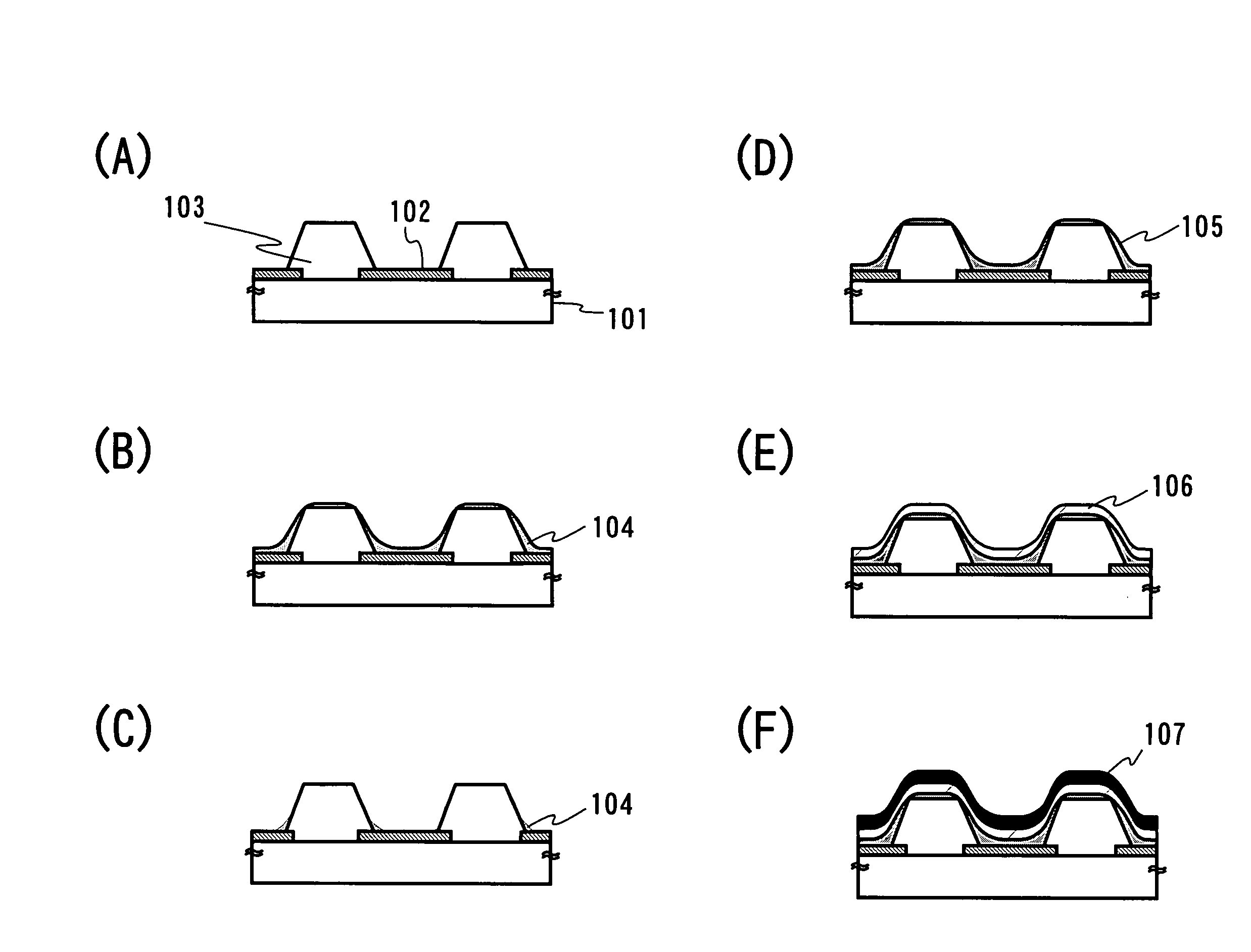
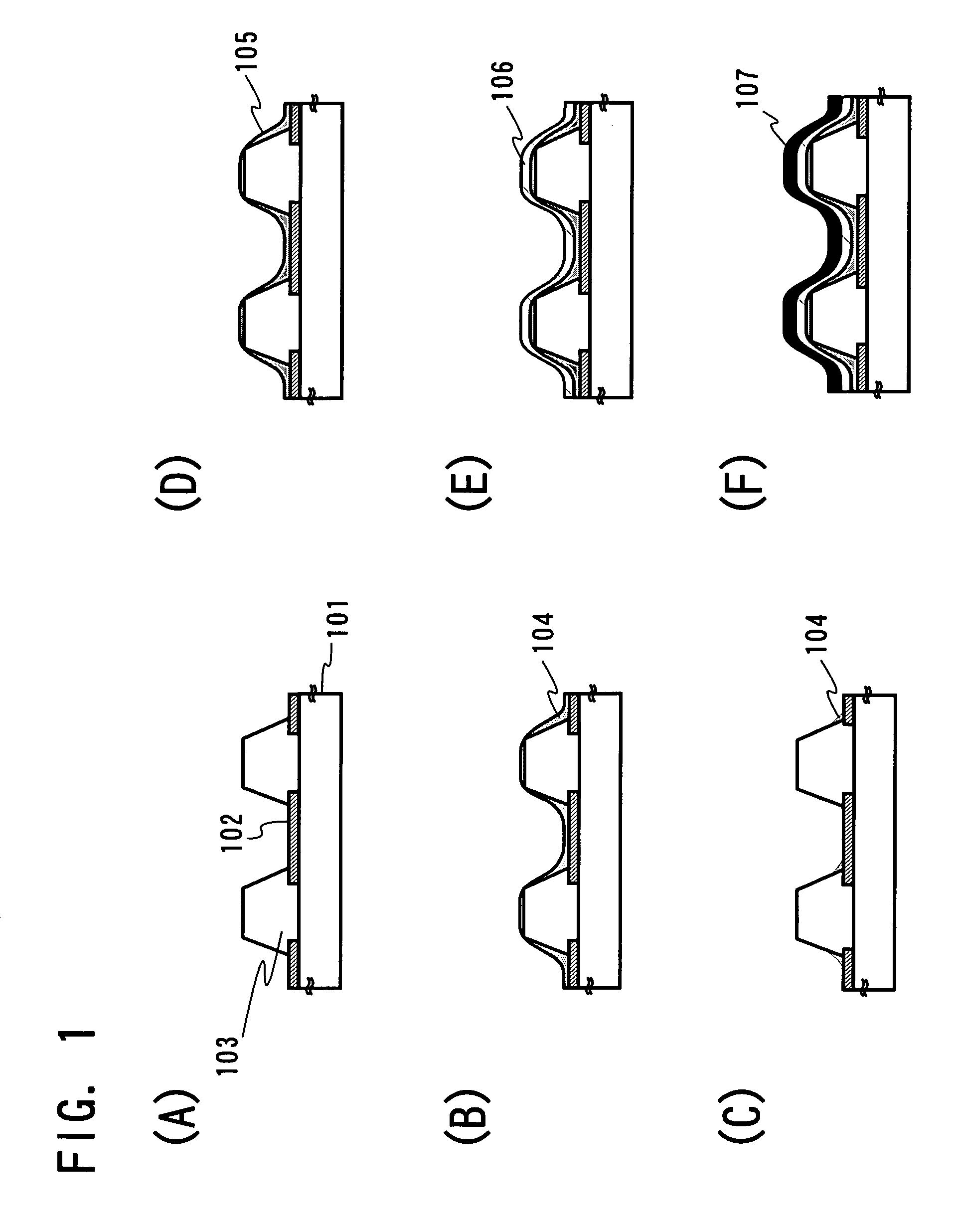
[0035]A schematic diagram of a method for manufacturing a display device of the present invention is shown in FIGS. 1(A) to 1(F) in the order corresponding to the steps while showing the cross sections. In FIG. 1(A), the one provided with a first electrode 102 on a substrate 101 and an insulating barrier 103 for surrounding the first electrode 102 is shown.

[0036]FIG. 1(B) shows a cross sectional view when the solution including an acceptor is applied over the substrate 101 in wet process as a first step. A solution layer 104 comprising the acceptor is formed on the first electrode 102 and the insulating barrier 103.

[0037]As for the acceptor, an organic compound having sulfonic acid group is preferable. For example, poly (styrenesulfonic acid) is given as an example, and further, aqueous solution is preferable for the solution including the acceptor.

[0038]Then, a cross sectional view after water is brought into contact over the substrate 101 as a second step is sho...

embodiment mode 2

(Embodiment Mode 2)

[0060]A metal which serves as an electron injection electrode (for example, AlLi alloy, MgAg alloy, or the like) is formed over the substrate by vacuum vapor deposition or EB method. Next, the solution including a donor is applied in wet process. As the donor, alkylammonium ion (for example, tetraethylammonium, tetrabutylammonium, or the like), or Tetrathiafulvalene (hereinafter referred to as “TTF”) are preferable. For the last, the conductive polymer including the donor is applied in wet process. As the conductive polymer, poly (aniline), poly (pyrrole) or the like is preferable.

[0061]The electroluminescent layer can be formed by vapor deposition or application in wet process. As the structure of the electroluminenscent layer, the structure of the light emitting element using the known organic EL material is preferably used. As an anode of the hole injection electrode, an ITO film is preferably used. The ITO film is preferably formed by sputtering, electron beam...

embodiment

(Embodiment 1)

[0062]FIG. 3(A) shows a substrate used in this embodiment. And FIG. 3(B) shows a cross sectional view of A–A′ in the drawing. An insulating barrier 303 is formed by photolithography over a glass substrate 301 on which a transparent electrode 302 of ITO is patterned. The transparent electrode 302 of the ITO is a rectangle with a film thickness of 100 nm and length of 300 μm and width of 60 μm. The insulating barrier 303 is formed from acrylic resin, which has 1.5 μm height.

[0063]In order to obtain the hydrophilic property of the transparent electrode 302 of ITO and the insulating barrier 303, UV ozone rinsing is carried out. Then, 1.5 wt % poly (styrenesulfonic acid) aqueous solution is spin coated. Pure water is applied to the substrate immediately, and the substrate is spun to cut the water. Lastly, PEDOT / PSS aqueous solution is applied over the entire surface so as to obtain the film thickness of 60 nm by spin coating, prebaked at 80° C. for 10 minutes, baked at 200°...


PUM

PropertyMeasurementUnit
thicknessaaaaaaaaaa
widthaaaaaaaaaa
lengthaaaaaaaaaa

Abstract

A method for manufacturing a display device of the present invention includes the steps of forming insulating barriers which surround electrode and project upward from the surface of the electrode, and bringing the whole substrate into contact with water after applying the solution including an acceptor in wet process. According to the present invention, an organic conductive layer can be uniformly formed over a substrate in wet process even if the substrate does not have a smooth surface and has distribution in wettability of the surface.

Description

TECHNICAL FIELD[0001]The present invention relates to a manufacturing method of a display device in which a display portion is formed from a light emitting element using an organic electroluminescent (hereinafter referred to as EL) material.BACKGROUND ART[0002]An display for displaying an image is one of essential information display mediums for modern life. The display for displaying an image is found as usage in several modes, such as starting from a so-called TV monitor, a liquid crystal display that has been rapidly developed recently, and an organic EL display that is expected the further development. Specifically, the liquid crystal display and the organic EL display are characterized by being able to drive in lower voltage, and are an important research and development issue in view of energy saving.[0003]Above all, the organic EL display attracts most attention as a next generation flat panel display.[0004]The emission mechanism of the light emitting element using an organic...

Claims


Application Information

Patent Timeline
Patent Type & Authority Patents(United States)
IPC IPC(8): H01J9/38H01L27/32H01L51/56H05B33/10H05B33/22
CPCH01L27/3246H01L51/0003H01L51/56H01L51/0012H01L51/5088H10K59/122H10K71/191H10K71/12H10K50/17H10K71/00
Inventor TOKUDA, ATSUSHI
Owner SEMICON ENERGY LAB CO LTD
Why Eureka
Try Eureka