Random access memory including nanotube switching elements

a technology of random access memory and switching elements, which is applied in the field of nanotube switching circuits, can solve the problems of high power consumption, density and operation speed of mos digital circuits, and limited density of bipolar digital integrated circuits

Active Publication Date: 2007-07-17
NANTERO
View PDF12 Cites 24 Cited by
  • Summary
  • Abstract
  • Description
  • Claims
  • Application Information

AI Technical Summary

Problems solved by technology

However, the density of bipolar digital integrated circuits is limited by their high power consumption and the ability of packaging technology to dissipate the heat produced while the circuits are operating.
The density and operating speed of MOS digital circuits are still limited by the need to dissipate the heat produced when the device is operating.
Digital logic integrated circuits constructed from bipolar or MOS devices do not function correctly under conditions of high heat or extreme environments.
As leakage current increases, the operating temperature of the device rises, the power consumed by the circuit increases, and the difficulty of discriminating the off state from the on state reduces circuit reliability.
Conventional digital logic circuits also short internally when subjected to certain extreme environments because electrical currents are generated inside the semiconductor material.
It is possible to manufacture integrated circuits with special devices and isolation techniques so that they remain operational when exposed to such environments, but the high cost of these devices limits their availability and practicality.
In addition, such digital circuits exhibit timing differences from their normal counterparts, requiring additional design verification to add protection to an existing design.
Integrated circuits constructed from either bipolar or FET switching elements are volatile.
Alternative solutions to avoid losing information in volatile digital circuits, such as battery backup, also add cost and complexity to digital designs.

Method used


Image

  • Random access memory including nanotube switching elements
  • Random access memory including nanotube switching elements
  • Random access memory including nanotube switching elements

Examples


Embodiment Construction

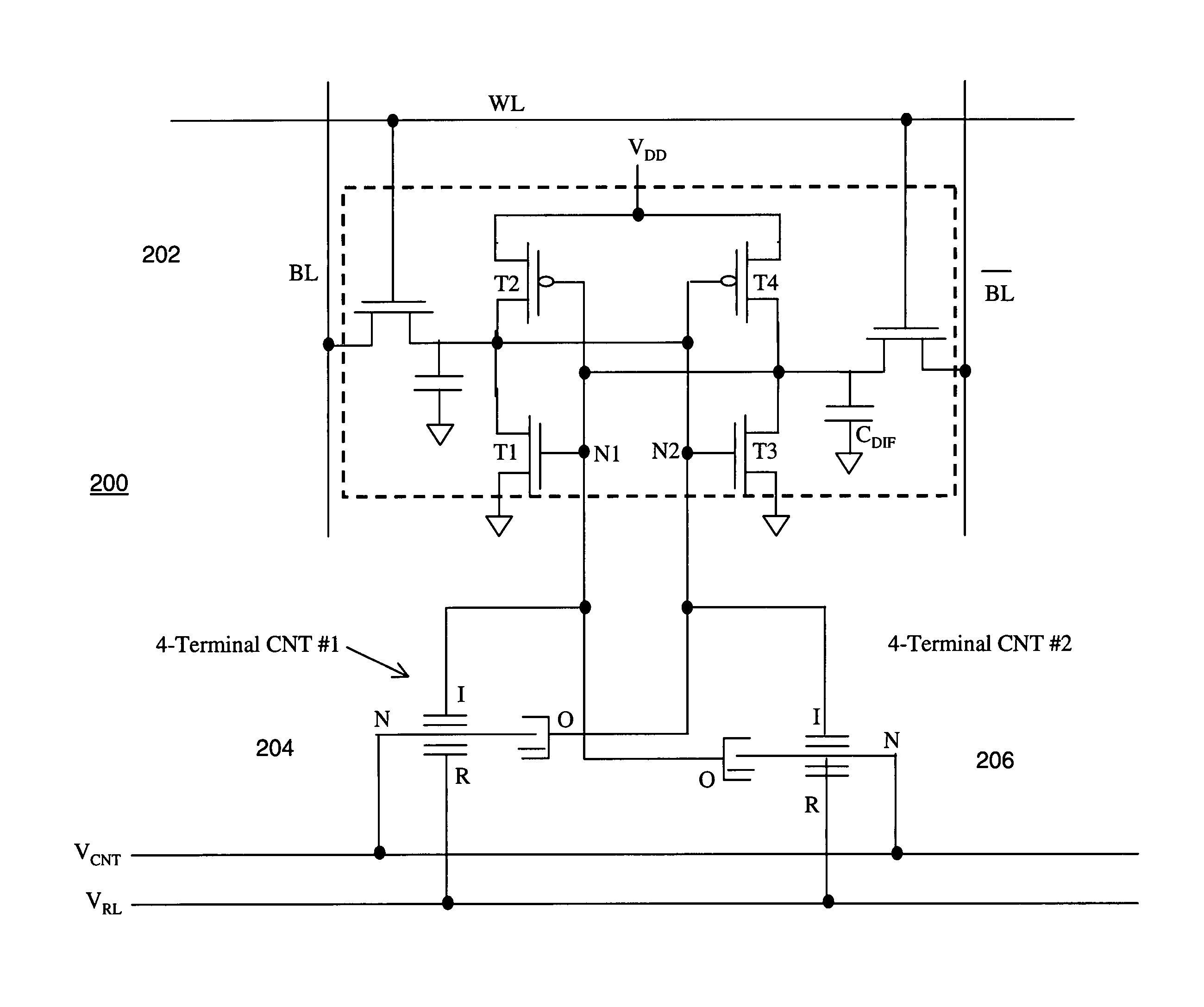
[0027]Preferred embodiments of the invention provide switching elements in which a nanotube-based switching element is included with an otherwise conventional RAM cell. The nanotube switching element may then be used to provide non-volatile storage functionality, for example, to act as a shadow ram. Moreover, the design of preferred embodiments of the nanotube switching elements may be included as extra layers on top of already formed RAM cells.

[0028]First, the nanotube switching element will be described. Second, the integration of such an element with a RAM cell will be explained.

Nanotube Switching Element

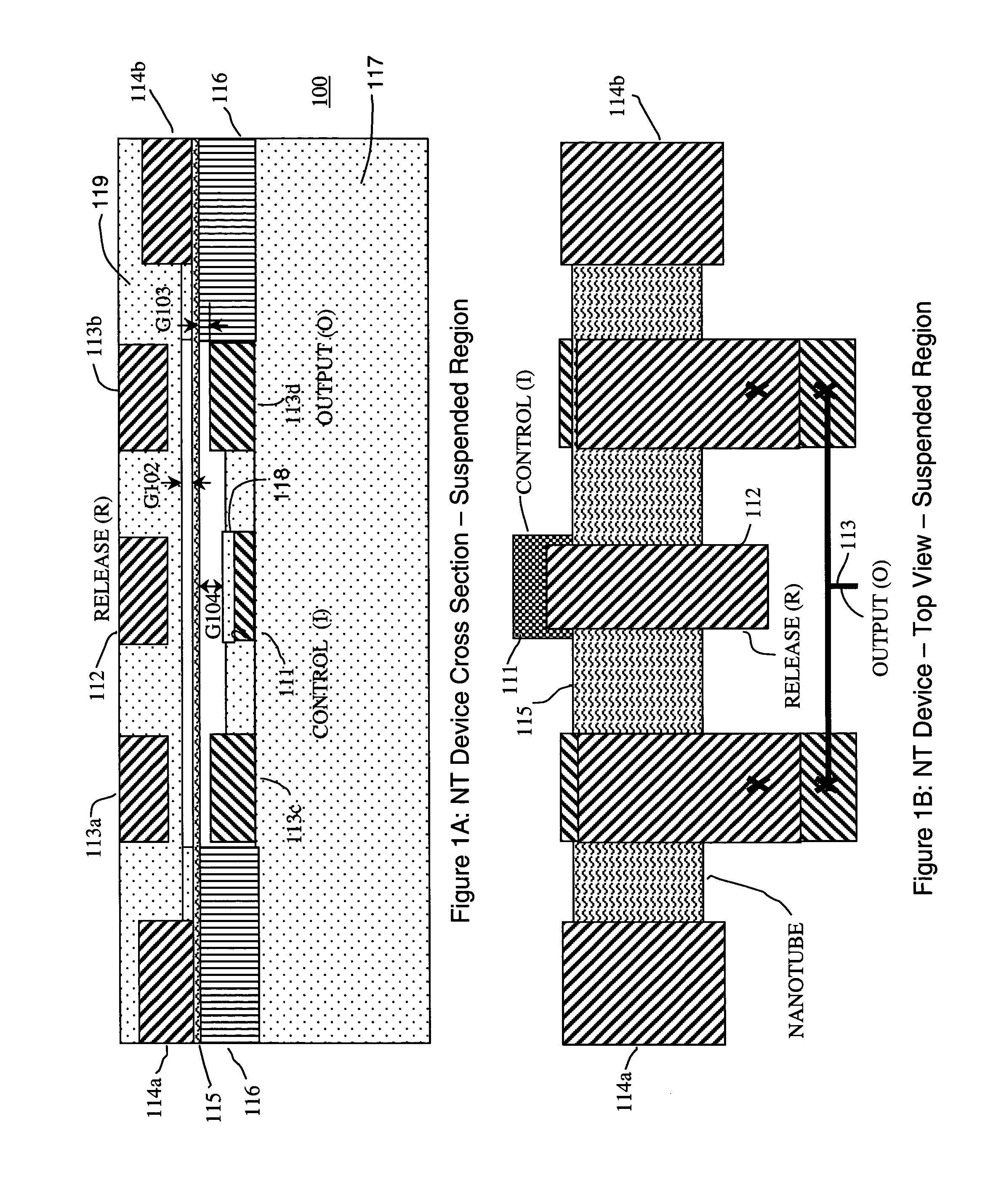
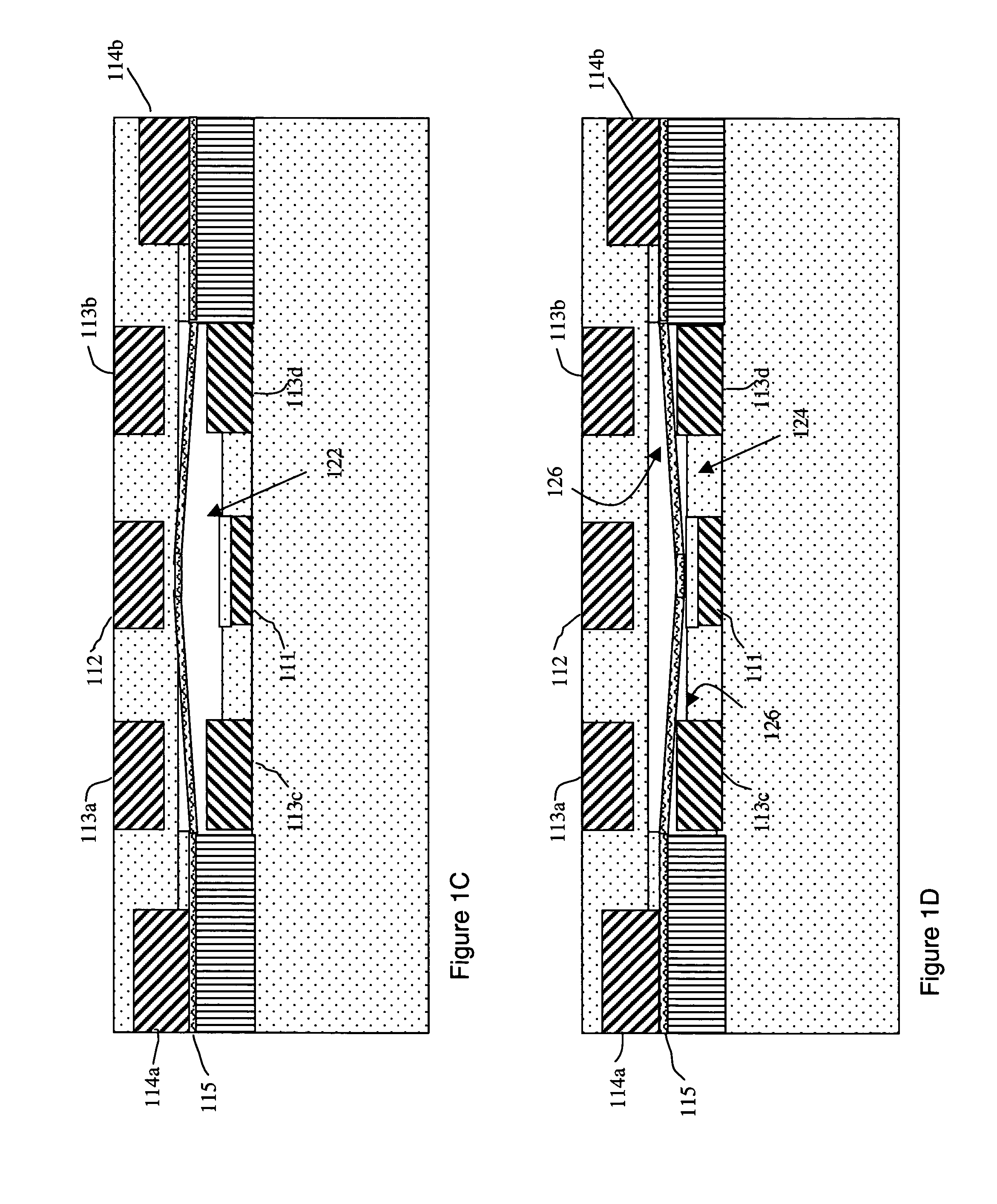
[0029]FIG. 1A is a cross sectional view of a preferred nanotube switching element 100. Nanotube switching element includes a lower portion having an insulating layer 117, control electrode 111, output electrodes 113c,d. Nanotube switching element further includes an upper portion having release electrode 112, opposing output electrodes 113a,b, and signal electrodes 114a,b. A nano...


PUM


Abstract

A random access memory cell includes first and second nanotube switching elements and an electronic memory with cross-coupled first and second inverters. Each nanotube switching element includes a nanotube channel element having at least one electrically conductive nanotube, and a set electrode and a release electrode disposed in relation to the nanotube channel element to controllably form and unform an electrically conductive channel between a channel electrode and an output node. Input nodes of the first and second inverters are coupled to the set electrodes and the output nodes of the first and second nanotube switching elements. The cell can operate as a normal electronic memory, or in a shadow memory or store mode to transfer the electronic memory state to the nanotube switching elements. The device may later be operated in a recall mode to transfer the state of the nanotube switching elements to the electronic memory.

Description

CROSS-REFERENCE TO RELATED APPLICATIONS[0001]This application claims priority under 35 U.S.C. § 119(e) to U.S. Provisional Pat. Apl. No. 60 / 612,300, filed on Sep. 22, 2004, entitled Random Access Memory Including Nanotube Switching Elements, which is incorporated herein by reference in its entirety.[0002]This application is a continuation-in-part and claims priority under 35 U.S.C. §120 to U.S. patent application Ser. No. 10 / 918,085, filed on Aug. 13, 2004, entitled Nanotube-Based Switching Elements With Multiple Controls, now U.S. Pat. No. 6,990,009, and hereby incorporates such reference in its entirety.BACKGROUND[0003]1. Technical Field[0004]The present application generally relates to nanotube switching circuits and in particular to nanotube switching circuits that can be used to provide non-volatile storage functionality to otherwise conventional random access memory (RAM).[0005]2. Discussion of Related Art[0006]Digital logic circuits are used in personal computers, portable el...

Claims


Application Information

Patent Timeline
Patent Type & Authority Patents(United States)
IPC IPC(8): G11C11/00B82B1/00G11C11/50G11C7/10
CPCB82Y10/00G11C13/025G11C14/00G11C23/00Y10S977/936Y10S977/733Y10S977/732Y10S977/943Y10S977/938
Inventor BERTIN, CLAUDE L.RUCKES, THOMASSEGAL, BRENT M.
Owner NANTERO
Why Eureka
Try Eureka