
Beam homogenizer, laser irradiation apparatus and method for manufacturing semiconductor device

a laser irradiation and laser beam technology, applied in the direction of photomechanical equipment, manufacturing tools, instruments, etc., can solve the problems of low melting point of synthetic quartz, problem in processing accuracy of each cylindrical lens, etc., and achieve the effect of wide margin of laser beam power, reduced loss of photoconduction, and high intensity

Inactive Publication Date: 2007-07-17
SEMICON ENERGY LAB CO LTD
View PDF54 Cites 30 Cited by
  • Summary
  • Abstract
  • Description
  • Claims
  • Application Information

AI Technical Summary

Benefits of technology

This approach results in stable and uniform crystallization of semiconductor films, reducing variations in electrical characteristics and enhancing the reliability of semiconductor devices, allowing for efficient mass production with improved yield and reduced manufacturing costs.

Problems solved by technology

On the other hand, the glass has a disadvantage that it has a lower melting point than the synthetic quartz.
When the cylindrical lens array is used, however, a processing accuracy of each cylindrical lens is a problem.
This can be a problem when performing the laser annealing to the semiconductor film.

Method used


Image

  • Beam homogenizer, laser irradiation apparatus and method for manufacturing semiconductor device
  • Beam homogenizer, laser irradiation apparatus and method for manufacturing semiconductor device
  • Beam homogenizer, laser irradiation apparatus and method for manufacturing semiconductor device

Examples


embodiment 1

[0060]The present embodiment explains an example using a different optical waveguide from that described in the embodiment mode with reference to FIGS. 4A and 4B.

[0061]In FIGS. 4A and 4B, the laser beam propagates in the direction indicated by an arrow. An optical waveguide 406 used in the present embodiment has a pair of reflection planes provided oppositely. In contrast with the optical waveguide 306 explained in FIGS. 3A and 3B, which is made of the medium having a refractive index of n (n>1) to occupy the region between the pair of reflection planes, the optical waveguide 406 in FIGS. 4A and 4B has a hollow space between the pair of reflection planes, which is filled with the air. The optical waveguides 306 and 406 are different in this point. In addition, the pair of reflection planes of the optical waveguide 406 is arranged so as to act in the direction of the minor axis of the rectangular beam according to the reason explained above. In a side view of FIG. 4A, the direction p...

embodiment 2

[0065]The present embodiment explains an example using the different optical system and the different optical waveguide from those described in the embodiment mode with reference to FIGS. 5A and 5B. In this embodiment, a fly-eye lens is used as a lens array. The fly-eye lens is different from the cylindrical lens array in that a plurality of spherical lenses is arranged in a matrix in the vertical plane with respect to the traveling direction of the laser beam. The optical waveguide 504 has two pairs of reflection planes provided oppositely with a region therebetween occupied by the synthetic quartz. Since the refractive index of the synthetic quartz is different from that of the air, the laser beam is reflected repeatedly in the optical waveguide 504. Specifically, in this case, because the synthetic quartz has higher refractive index than the air, the laser beam is totally reflected in the optical waveguide 504 repeatedly at a critical angle or more, and reaches the exit.

[0066]In ...

embodiment 3

[0069]The present embodiment explains an example using the different optical waveguide from that described in the embodiment mode with reference to FIGS. 6A and 6B. In FIGS. 6A and 6B, a cylindrical lens array 602 is used as a lens array. An optical waveguide 606 has two pairs of reflection planes provided oppositely with a region therebetween occupied by the synthetic quartz. Since the synthetic quartz has higher refractive index than the air, the laser beam incident into the optical waveguide 606 is totally reflected repeatedly and reaches the exit.

[0070]In FIGS. 6A and 6B, the laser beam emitted from a laser oscillator 601 propagates in the direction indicated by an arrow. Firstly, a side view of FIG. 6A is explained. In the side view of FIG. 6A, the direction perpendicular to the paper is the direction of the major axis of the rectangular beam. The laser beam is incident into a cylindrical lens array 602, and is divided in the direction of the minor axis of the rectangular beam....


PUM

PropertyMeasurementUnit
refractive indexaaaaaaaaaa
lengthaaaaaaaaaa
lengthaaaaaaaaaa

Abstract

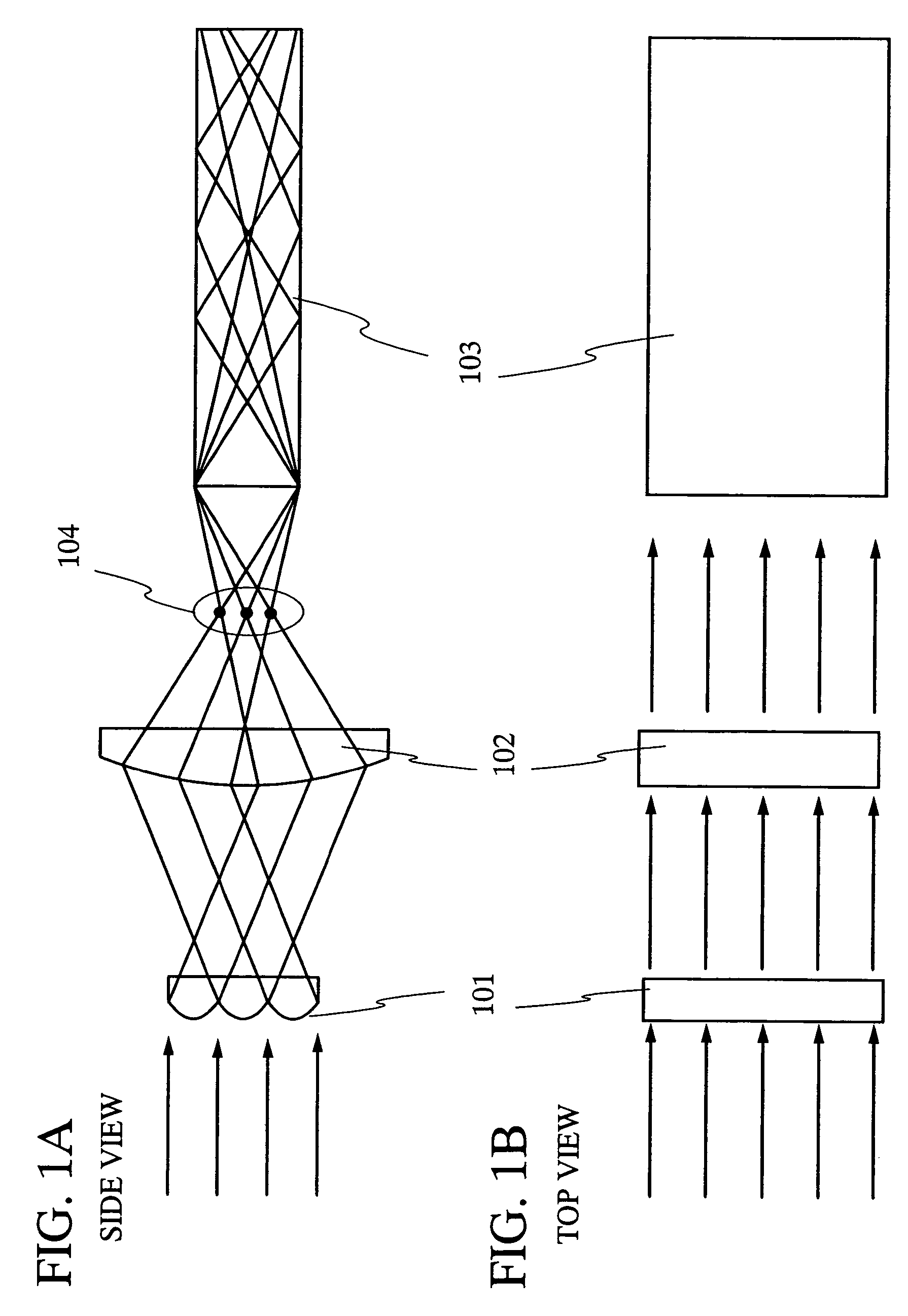
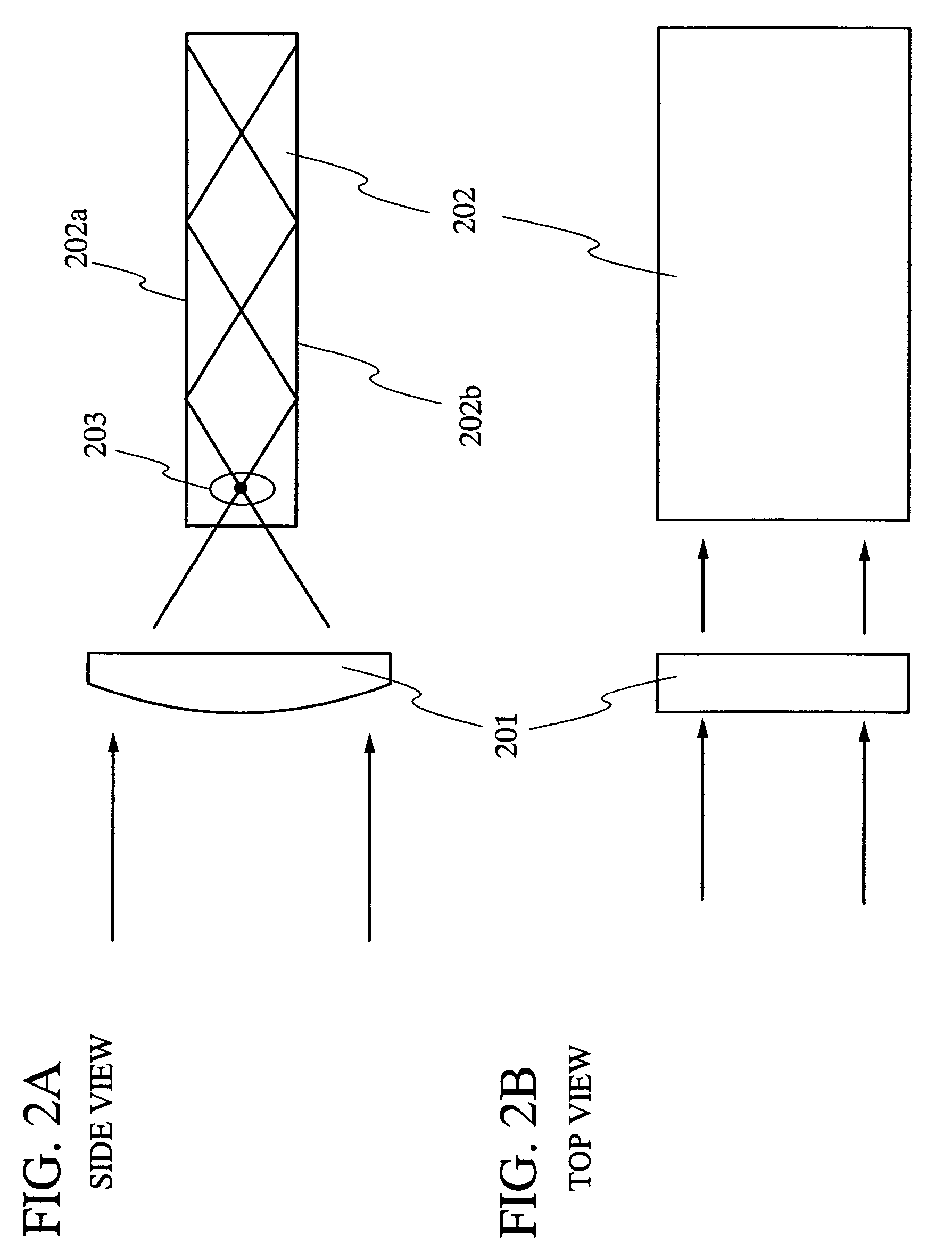
A cylindrical lens array cannot be manufactured so that each cylindrical lens has the same radius of curvature and the same accuracy in the surface. Therefore, when the laser annealing is performed using the cylindrical lens array, the beam spots divided by the cylindrical lens array cannot be superposed completely in the same surface. As a result, there is a region where the energy is attenuated in the edge portion of the rectangular beam to be formed, and therefore the intensity distribution of the laser beam becomes inhomogeneous. In the present invention, the cylindrical lens array is used in combination with the optical waveguide. After dividing the laser beam in a predetermined direction by the cylindrical lens array, the divided beams are combined, and then the laser beam is incident into the optical waveguide that acts upon the same direction as the predetermined direction. This can correct the variation in the intensity of the laser beam due to the processing inaccuracy of the cylindrical lens array.

Description

BACKGROUND OF THE INVENTION[0001]1. Field of the Invention[0002]The present invention relates to a beam homogenizer for homogenizing intensity distribution of a laser beam in a particular region of an irradiated surface. In addition, the present invention relates to a laser irradiation apparatus for irradiating the laser beam to the irradiated surface. Furthermore, the present invention relates to a method for manufacturing a semiconductor device having a crystalline semiconductor film formed using the laser irradiation apparatus.[0003]2. Related Art[0004]In recent years, a method for manufacturing a crystalline semiconductor film by irradiating a laser beam to a non-single crystal semiconductor film formed over a glass substrate has been extensively employed (this method is hereinafter referred to as laser annealing). It is noted that the term “crystalline semiconductor film” herein used means a semiconductor film having a crystallized region, and includes a semiconductor film havi...

Claims


Application Information

Patent Timeline
Patent Type & Authority Patents(United States)
IPC IPC(8): G02B6/26G02B6/00B23K26/06H01S5/10B23K26/067B23K26/073G02B6/42G02B27/09G03F7/20H01L21/26H01S3/00
CPCB23K26/0604B23K26/067B23K26/0732G02B6/4206G02B27/0927G02B27/0994G03F7/70075H01S3/005B23K2201/40B23K2101/40H01S5/10H01L21/26
Inventor TANAKA, KOICHIRO
Owner SEMICON ENERGY LAB CO LTD
Learn More