

Deposition method of TiN thin film having a multi-layer structure
a technology of metal nitride and multi-layer structure, which is applied in the direction of coating, chemical vapor deposition coating, metallic material coating process, etc., can solve the problems of high specific resistance and impurity content, quick change of resistance, and deterioration of device properties, so as to improve stability, increase the pattern aspect ratio, the effect of reducing the deposition temperatur
- Summary
- Abstract
- Description
- Claims
- Application Information
AI Technical Summary
Benefits of technology
Problems solved by technology
Method used
Image

Examples
Embodiment Construction
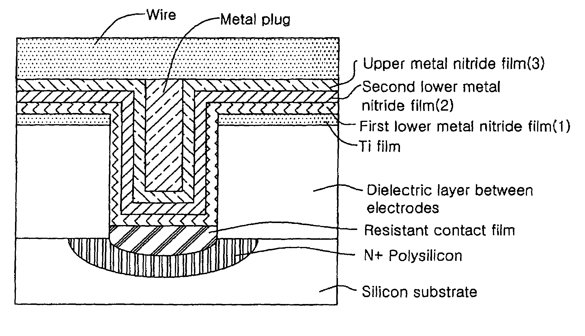
[0016]The methods of depositing a metal nitride film according to embodiments of the present invention are described in FIGS. 1 through 4. A core thin film deposition method is described. The concept of an apparatus for depositing a thin film to embody the present invention is illustrated in FIGS. 5 and 6. Also, examples of the present invention applied to a semiconductor devices are illustrated in FIGS. 7 and 8.
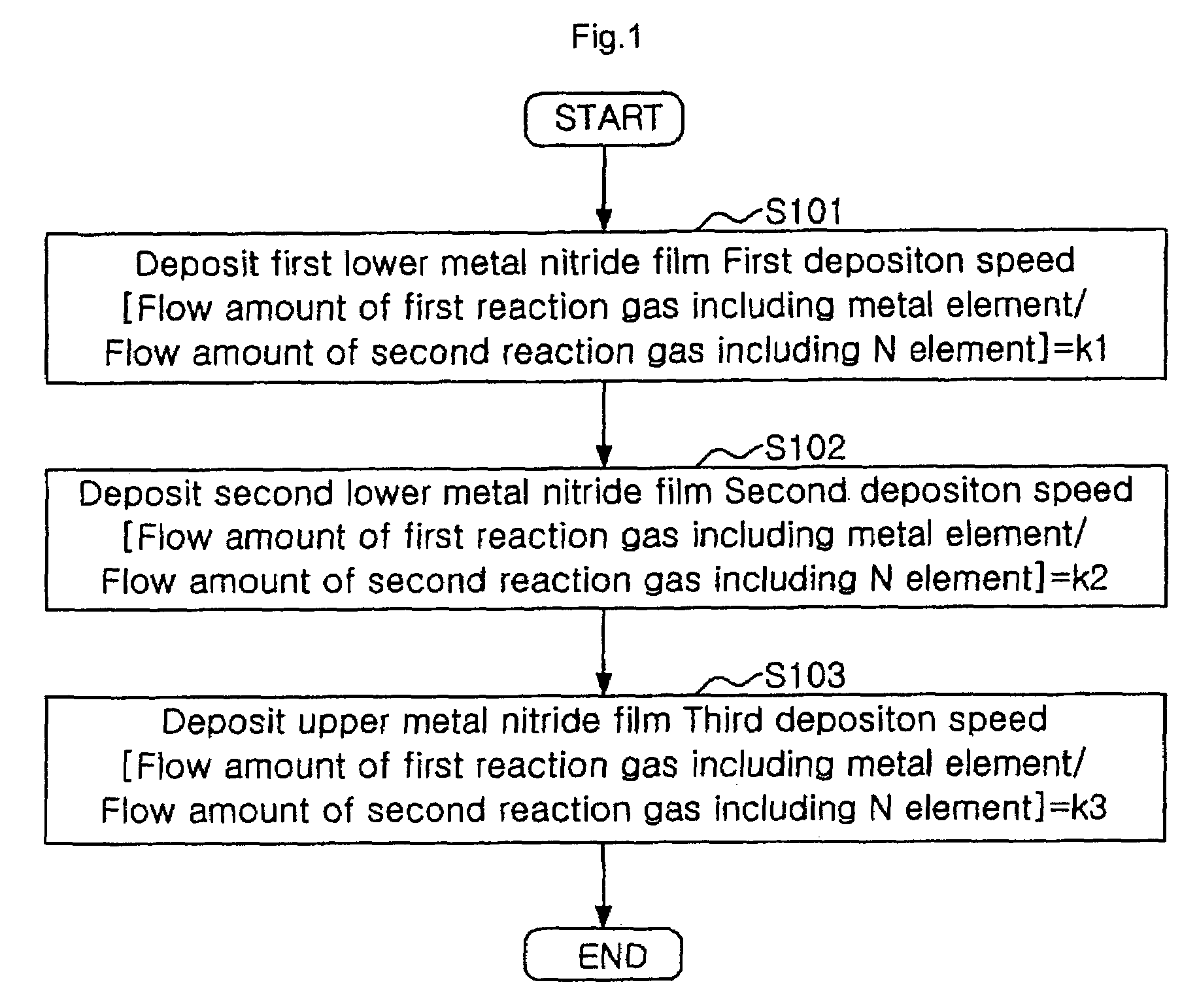
[0017]FIG. 1 is a flow chart for explaining the principle of a method of depositing a metal nitride film having a multilayer structure according to the present invention.
[0018]In the process of depositing a metal nitride film of a semiconductor device, the present invention is suggested as one of methods to maximize step coverage and stability with respect to the exposure to air / moisture without deterioration of its property when deposited on a pattern having a narrow aspect ratio at a low temperature.
[0019]The fundamental principle of the present invention is to deposit a m...
PUM
| Property | Measurement | Unit |
|---|---|---|
| structure | aaaaa | aaaaa |
| stability | aaaaa | aaaaa |
| deposition speed | aaaaa | aaaaa |
Abstract
Description
Claims
Application Information