Method and apparatus for solution processed doping of carbon nanotube

a technology of carbon nanotubes and solutions, applied in the field of nanostructures, can solve the problems of large variation in carbon nanotube fets, no known method for reliably preparing carbon nanotubes having particular characteristics, and too high device threshold voltages for ultimate device scaling

a technology of carbon nanotubes and solutions, applied in the field of nanostructures, can solve the problems of large variation in carbon nanotube fets, no known method for reliably preparing carbon nanotubes having particular characteristics, and too high device threshold voltages for ultimate device scaling

US7253431B2Active Publication Date: 2007-08-07GLOBALFOUNDRIES U S INC

Image

  • Method and apparatus for solution processed doping of carbon nanotube
  • Method and apparatus for solution processed doping of carbon nanotube
  • Method and apparatus for solution processed doping of carbon nanotube

Examples


Embodiment Construction

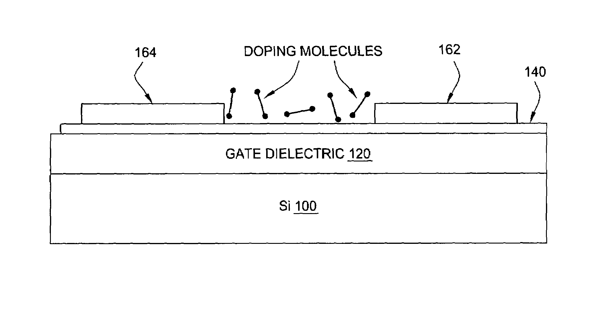
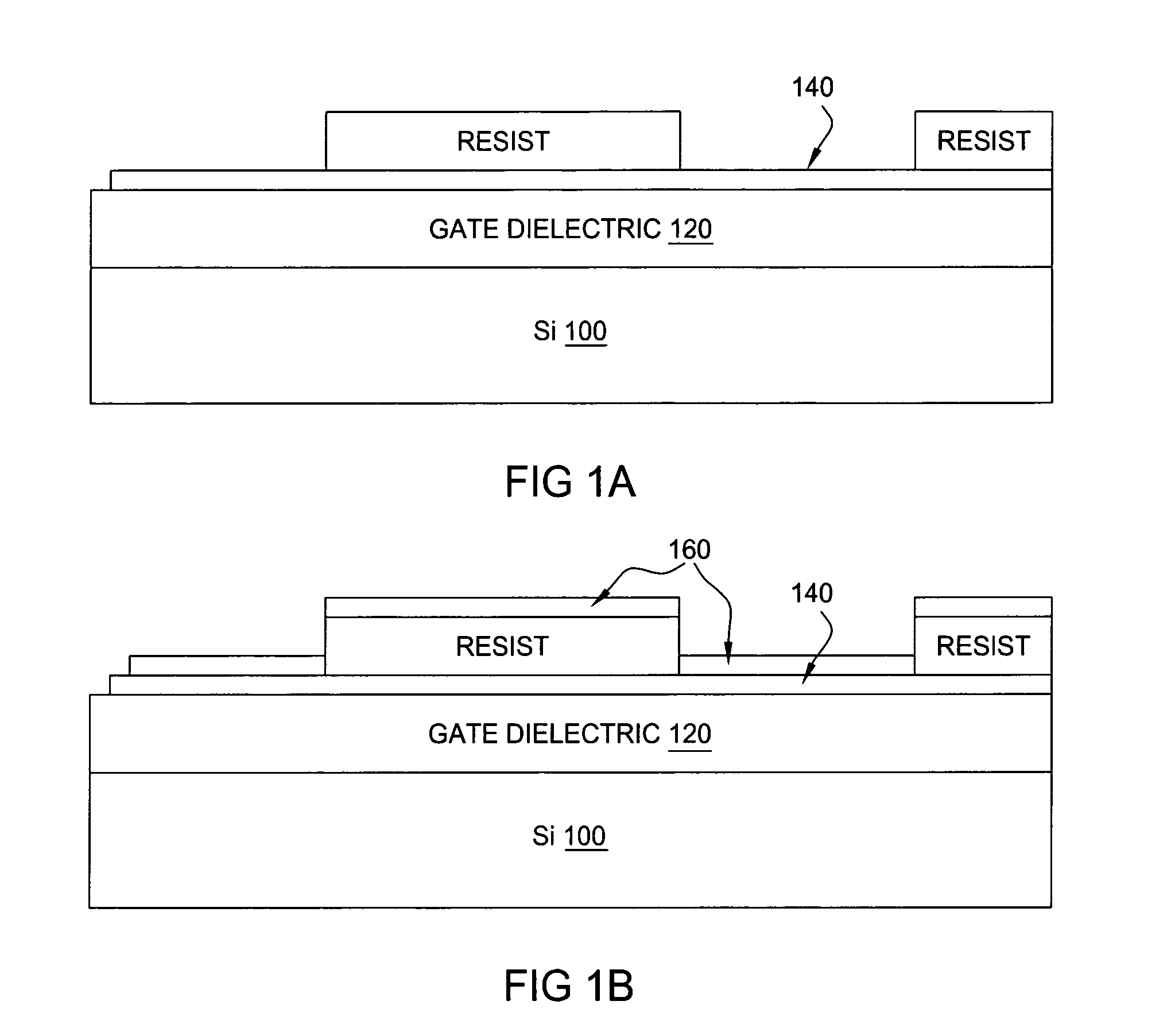
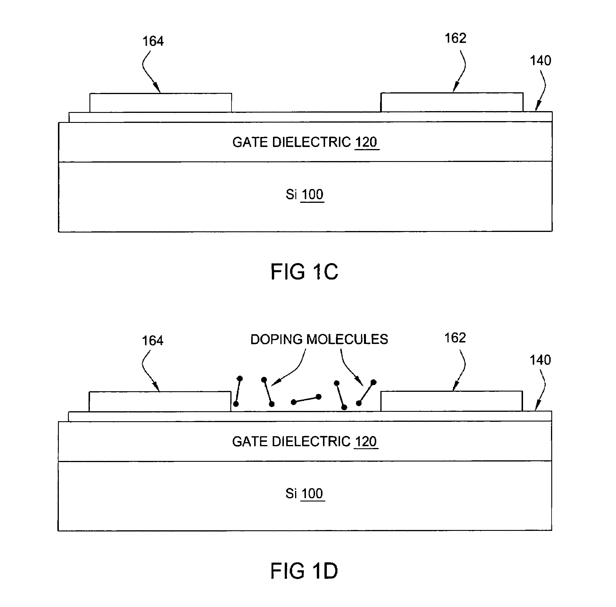
[0022]In one embodiment, the present invention relates to a method for forming a carbon nanotube which has been doped by solution processing. The carbon nanotubes of the invention are air-stable and exhibit improved device performance in both on- and off-states. Characteristics of the carbon nanotube of the invention include without limitation, tunability of the threshold voltage Vth, an improved Ion by about 1 to about 3 orders of magnitude, a suppressed minority carrier injection and immunity from drain induced Ioff degradation from regular SB carbon nanotube FET which in the case of carbon nanotube FET, transforms carbon nanotube FET from ambipolar to unipolar, a ratio of Ion / Ioff ratio of about 102 to about 107 and drain induced barrier lowering (DIBL) like behavior. Ion is defined as the current when the transistor is switched on (Vg>Vth). One usually compares Ion at a constant overdrive (i.e., Vg-Vth=constant, e.g., around 0.5V.

[0023]According to one embodiment of the present ...


PUM

PropertyMeasurementUnit
temperatureaaaaaaaaaa
threshold voltageaaaaaaaaaa

Abstract

A method is provided for doping a carbon nanotube. The method comprises exposing the nanotube to a one-electron oxidant in a solution phase. A method is also provided for forming a carbon nanotube FET device.

Description

CROSS-REFERENCE TO RELATED APPLICATION[0001]This application claims priority from Provisional Application Ser. No. 60 / 549,185 filed Mar. 2, 2004, which is herein incorporated by reference.BACKGROUND[0002]The present invention relates to nanostrutures and particularly to solution processing methods for doping a carbon nanotube (CN).[0003]In the field of molecular nanoelectronics, few materials show as much promise as nanotubes, and in particular carbon nanotubes, which comprise hollow cylinders of graphite. Nanotubes are made into tiny electronic devices such as diodes and transistors, depending on the electrical characteristics of the nanotube. Nanotubes are unique for their size, shape, and physical properties. Structurally a carbon nanotube resembles a hexagonal lattice of carbon rolled into a cylinder.[0004]Besides exhibiting intriguing quantum behaviors at low temperature, carbon nanotubes exhibit at least two important characteristics: a nanotube can be either metallic or semic...

Claims


Application Information

Patent Timeline
07 Aug 2007
Publication
US7253431B2
IPC
H01L29/06
CPC
B82Y10/00; B82Y30/00; H01L51/002; H01L51/0048; H01L51/0541; H01L51/0545; Y10S977/938; Y10S977/749
Inventors
AFZALI-ARDAKANI, ALI; AVOURIS, PHAEDON