Method for processing graphene-carbon nanotube FET device

A graphene nanoribbon and carbon nanotube technology, applied in nanotechnology, semiconductor devices, electrical components and other directions, can solve the problems of easily contaminated samples, low precision, harsh operating environment, etc., and achieve low cost, high precision, and robustness. strong effect

Active Publication Date: 2018-12-21
PINGDINGSHAN UNIVERSITY
View PDF2 Cites 7 Cited by
  • Summary
  • Abstract
  • Description
  • Claims
  • Application Information

AI Technical Summary

Problems solved by technology

When it is necessary to process paired graphene nanoelectrodes with nanoscale gaps, most of the existing me

Method used


Image

  • Method for processing graphene-carbon nanotube FET device
  • Method for processing graphene-carbon nanotube FET device
  • Method for processing graphene-carbon nanotube FET device

Examples


Embodiment Construction

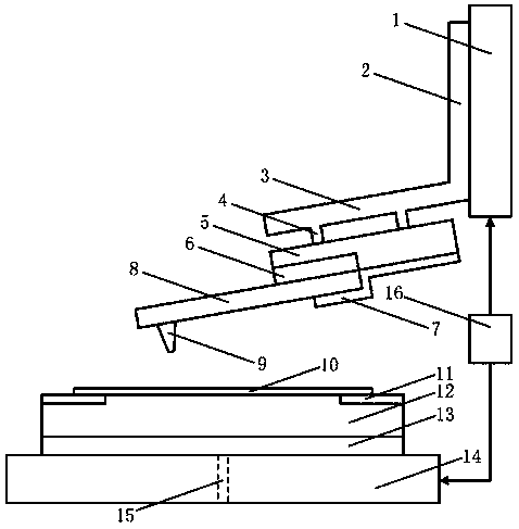
[0044] Such as Figure 1-Figure 6 Shown, the processing method of graphene-carbon nanotube FET device of the present invention, comprises the following steps,

[0045] (1), assembling the graphene sheet 10 on the cutting processing system;

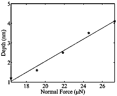
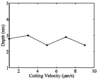
[0046] (2) Set the cutting force, cutting speed and cutting path for the cutting processing system;

[0047] (3) Start the cutting and processing system to cut and process the graphene sheet 10 into graphene nanoribbons 19;

[0048] (4), cutting off the graphene nanoribbon 19, and processing the graphene nanoelectrode whose electrode front end width and electrode pair gap are nanoscale;

[0049] (5) Establish a force model of single-walled carbon nanotubes in a non-uniform electric field;

[0050] (6) Remove the graphene nano-electrode from the cutting processing system and place it on the circular sample platform 24 and fix it under negative pressure, titrate the single-walled carbon nanotube solution after the graphene nano-electrode ...


PUM


Abstract

A method for processing graphene-carbon nanotube FET device comprises the following steps of: (1) assembling a graphene sheet on a cutting processing system; (2) setting cutting force, cutting speed and cutting path to the cutting processing system; (3) cutting the graphene sheet into graphene nanobelts; (4) processing a graphene nano-electrode; (5) establishing a stress model of a single-walled carbon nanotube in a non-uniform electric field; (6) titrating the single-walled carbon nanotube solution into the nano gap after the graphene nano-electrode is cut off. The processing method has the advantages of high precision, strong robustness, simple operation, flexibility and low cost. The processed graphene nano-electrode with the nano gap can be used as a probe for the nano point electricalproperty test and the detection of the biological molecules in a micro-environment, has higher sensitivity, and provides a new way for constructing micro-nano electronic equipment with smaller sizesand higher performances.

Description

technical field [0001] The invention belongs to the technical fields of micro-nano processing and micro-nano assembly, and in particular relates to a processing method of a graphene-carbon nanotube FET device. Background technique [0002] Nanoelectrodes are a newly developed field in electrochemical research. Due to its incomparable advantages with conventional electrodes: high mass transfer rate, small time constant, high signal-to-noise ratio, high current density, nano-electrodes are widely used in nano-biosensors, single-cell analysis, imaging probes, electrochemical kinetics research and other fields. When the gap between the electrode pairs reaches the nanometer level, the electrodes are also called nano-gap electrodes. Nano-gap electrodes are the basis for constructing nanoscale circuits and devices. Effective tool. Therefore, exploring new nano-electrode materials and developing nano-electrode processing methods with nano-gap has important theoretical research an...

Claims


Application Information

Patent Timeline
IPC IPC(8): B82Y40/00H01L29/40H01L29/772
CPCB82Y40/00H01L29/40H01L29/772
Inventor 解双喜秦莉莉王亚锋贠革鑫孔振威李光喜陈凡曹森鹏赵志敏代克杰
Owner PINGDINGSHAN UNIVERSITY
Why Eureka
Try Eureka