Light-emitting-diode chip comprising a sequence of GaN-based epitaxial layers which emit radiation and a method for producing the same

a technology of light-emitting diodes and epitaxial layers, which is applied in the direction of basic electric elements, electrical apparatus, semiconductor devices, etc., can solve the problem of high back-reflection of incident electromagnetic radiation into the chip, and achieve the effect of improving heat dissipation, reducing additional production expenditure, and improving current spread

Inactive Publication Date: 2007-09-04
OSRAM OLED
View PDF119 Cites 99 Cited by
  • Summary
  • Abstract
  • Description
  • Claims
  • Application Information

AI Technical Summary

Benefits of technology

[0007]The object of the invention is, first, to develop an LED chip of the type cited at the beginning hereof that offers improved current spread and whose additional production expenditure is kept to a minimum. An LED component with improved heat dissipation from the active region is also to be provided.

Problems solved by technology

This results in high back-reflection of the incident electromagnetic radiation into the chip.

Method used


Image

  • Light-emitting-diode chip comprising a sequence of GaN-based epitaxial layers which emit radiation and a method for producing the same
  • Light-emitting-diode chip comprising a sequence of GaN-based epitaxial layers which emit radiation and a method for producing the same

Examples


Embodiment Construction

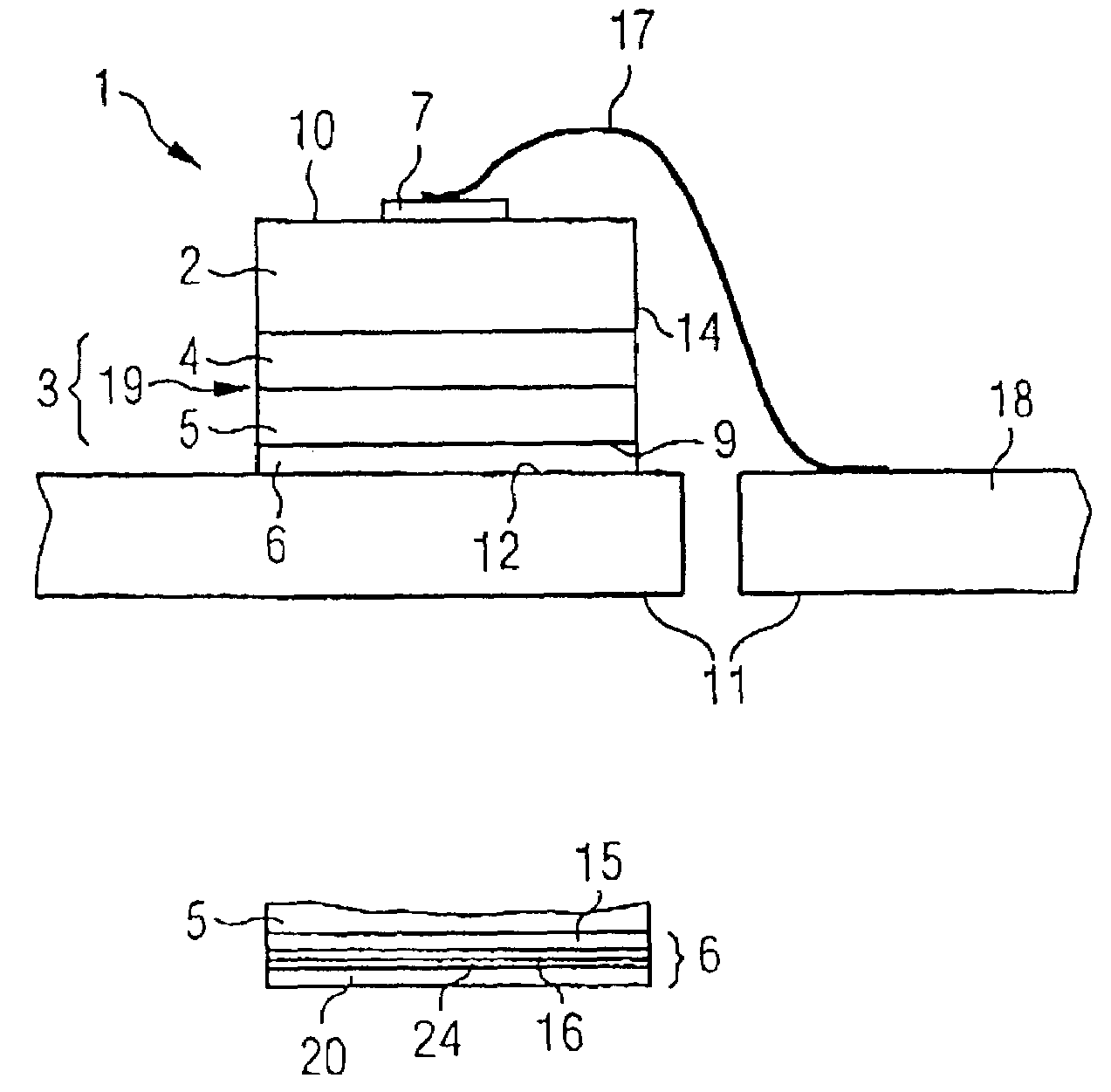
[0027]In the LED chip 1 of FIG. 1a, deposited on an SiC substrate 2 is a radiation-emitting epitaxial layer sequence 3. The latter is composed of an n-type doped GaN or AlGaN epitaxial layer 4 and a p-type doped GaN or AlGaN epitaxial layer 5. There can equally well be provided, for example, a GaN-based epitaxial layer sequence 3 having a double heterostructure, a single quantum well (SQW) structure or a multi-quantum well (MQW) structure comprising one or more undoped layer(s) 19, for example of InGaN or InGaAlN.

[0028]The SiC substrate 2 is electrically conductive and is transparent to the radiation emitted by an active region 19 of the epitaxial layer sequence 3.

[0029]Deposited with substantially full area coverage on epitaxial layer sequence 3, on its p-side 9 facing away from SiC substrate 2, is a reflective, bondable, Ag-based contact metallization 6. This is, for example, composed substantially of Ag, a PtAg alloy and / or a PdAg alloy.

[0030]As shown schematically in FIG. 1b, ho...


PUM


Abstract

A light-emitting diode chip (1) comprises a GaN-based, radiation-emitting epitaxial layer sequence (3), an active region (19), an n-doped layer (4) and a p-doped layer (5). The p-doped layer (5) is provided, on its main surface (9) facing away from the active region (19), with a reflective contact metallization (6) comprising a radioparent contact layer (15) and a reflective layer (16). Methods for fabricating LED chips of this type by thin-film technology are provided, as are LED components containing such LED chips.

Description

FIELD OF THE INVENTION[0001]The invention relates to a light-emitting diode chip comprising a GaN-based, radiation-emitting epitaxial layer sequence, to a method for fabricating the same, and to a light-emitting diode component comprising a light-emitting diode chip of this type.BACKGROUND OF THE INVENTION[0002]The term “GaN-based” as used herein encompasses in particular all ternary and quaternary GaN-based mixed crystals, such as AlN, InN, AlGaN, InGaN, InAlN and AlInGaN and gallium nitride itself.[0003]A fundamental problem in the fabrication of GaN-based light-emitting diode (LED) chips is that the maximum attainable electrical conductivity of p-doped layers, especially p-doped GaN or AlGaN layers, is not sufficient to achieve current spread over the entire lateral cross section of the chip with conventional front contact metallization, as known from LED chips made of other material systems (to maximize radiation decoupling, this type of metallization covers only a fraction of t...

Claims


Application Information

Patent Timeline
Patent Type & Authority Patents(United States)
IPC IPC(8): H01L33/00H01L33/40
CPCH01L33/0079H01L33/405H01L2224/48091H01L2224/73265H01L2924/00014H01L2924/01067H01L2924/12041H01L2224/32225H01L2224/48227H01L2924/00012H01L24/73H01L33/0093H01L33/32H01L33/42
Inventor HAHN, BERTHOLDJACOB, ULRICHLUGAUER, HANS-JURGENMUNDBROD-VANGEROW, MANFRED
Owner OSRAM OLED
Why Eureka
Try Eureka